Optoelectronic Devices and Properties
The operational characteristics of these circuits are studied, by simulations, using circuit
simulation software (e.g. Multisim). Following that, we investigate the influence of various
circuit parameters to the complexity of the so generated strange attractors. From the
obtained -calculated and recorded- time series, we estimate, with non-linear analysis, the
invariant parameters, as correlation, embedding dimension, Kolmogorov entropy and
Lyapunov exponents, of the corresponding strange attractors as function of the control
parameters.
2. RL-LED optoelectronic circuits
2.1 Circuit’s description
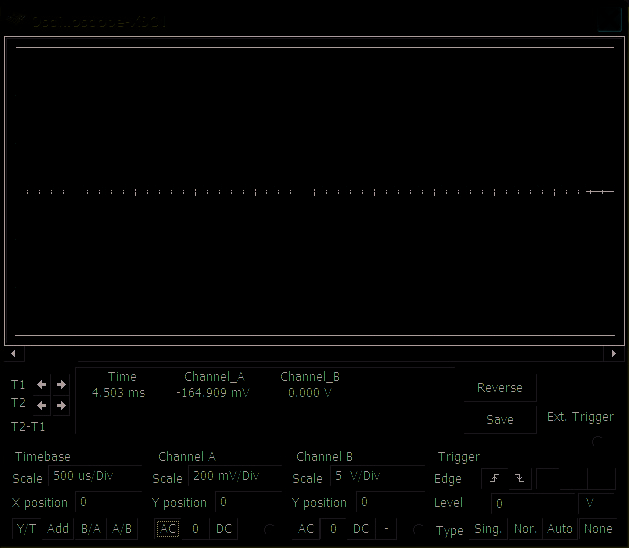
A non autonomous chaotic circuit driven RL-LED circuit (Hanias et al., 2008) is shown in
Figure 1. It consists of a series connection of an ac-voltage source, a linear resistor R1, a linear
inductor L1 and a typical LED. The value of R1 100 Ω and inside the circuits has been placed
in series with the LED. In the circuit’s input has been applied a sinusoidal voltage with
amplitude V1 as applied through an inductor L1 with value 47mH. The simulated circuit
operation is monitored by checking the voltage value across resistor R1. In Figure 2 is shown
the, obtained by the simulation, chaotic time series at the output for input signal’s amplitude
V1,rms = 7V and frequency f=10 KHz.
47mH
XSC1
IC=0A
LED1
G
V1
10% L1
T
7 Vrms
A
B
10kHz
Probe1,Probe1
0Deg
R1
100?
10%
V: 2.38 V
V(p-p): 16.5 V
V(rms): 7.72 V
V(dc): -13.7 mV
I : -248 uA
I (p-p): 4.26 mA
I (rms): 2.58 mA
I (dc): 1.78 mA
Freq.: 19.7 kHz
Fig. 1. RL-LED chaotic circuit in Multisim circuits simulation software
Optoelectronic Chaotic Circuits
633
Fig. 2. Chaotic signal V= V(t) across resistor R1 for the RL-LED circuit of Figure 1
2.2 Non-linear analysis
Next, we proceed to the analysis of the obtained chaotic time series following the method
proposed by Grassberger and Procaccia (Grassberger & Procaccia, 1983) and successfully
applied in similar cases (Hanias & Anagnostopoulos, 1993). Additionally, according the
Takens theory (Takens, 1981), the measured time series can be used to reconstruct the
original phase space. At first, we calculate the correlation integral C(r) for the simulated
output signal, for lim(r)=0 and lim(N)=∞ ( Ν represents the number of the corresponding
time series points), as defined by Kantz and Schreiber (Kanz & Schreiber, 1997):
N
G
G
1
C( r) =
∑ H( r − X − X (1)
l
j )
N
l=1,
pairs j= l+ W
where W is the Theiler window (Kanz and Schreiber, 1997), Η is the Heaviside function, and
Npairs is given as:
634
Optoelectronic Devices and Properties
2
N
=
(2)
pairs
( N − m + 1)( N − m + W + 1)
with m being the embedding dimension. It is clear that the summation in (1) counts the
G G
G
G
number of pairs ( X X for which the distance, i.e. the Euclidean norm X − X is less
l ,
j )
l
j
than r in an m dimensional Euclidean space. Here, the number of the experimental points is
G
N=10896, while, considering the m dimensional space, each vector X will be given as,
l
G
X = { V ( t ), V ( t +τ ), V ( t + τ
2 ),…, V( t + ( m − 1 τ) }
) (3)
l
i
i
i
i
and represents a point of the m dimensional phase space in which the attractor is embedded
each time. In equation (3), τ is the delay time factor determined by the first minimum of the
mutual information function I(τ) and defined as τ=A Δt with A=1,2,…,N where Δt=6.25μs is the sample rate. As shown in Figure 3, in our case, the mutual information function I(τ)
exhibits a local minimum at τ=5 time steps and thus we consider this value as the optimum
one.
2.0
1.5
I
1.0
0.5
0.0
0
5
10
15
20
τ
Fig. 3. Average mutual information I(τ) versus delay time τ
Next, we investigate the parameter W which is the Theiler window. As Theiler pointed out
if temporally correlated points are not neglected, spuriously low dimension estimate may be
Optoelectronic Chaotic Circuits
635
obtained (Stelter & Pfingsten, 1991). However, since there is no concrete rule of how to
choose W, it may take the first zero-crossing value of the correlation function CR(τ) (Kanz &
Schreiber, 1997), as suggested by Kantz and Schreiber (Kanz & Schreiber, 1997). This means
that we can use the correlation length as a starting value for W. As shown in Figure 4, the
correlation length is equal to 5 and thus, W= 5 time lags. Figure 4 also depicts a strong
correlation between the data indicating the way past states affect the system’s current state.
Hence, we can use these values for phase space reconstruction.
1.2
1.0
0.8
0.6
0.4
τ)
0.2
CR(
0.0
-0.2
-0.4
-0.6
-0.8
0
2
4
6
8
10
12
14
16
18
20
τ
Fig. 4. Correlation function CR(τ) versus delay time τ
It has been proven (Grassberger & Procaccia, 1983) that if the attractor is a strange one, the
correlation integral will be proportional to rν, where v is a measure of the attractor’s
dimension called correlation dimension. By definition, the correlation integral C(r) is the
limit of correlation sum of equation (1) and is numerically calculated as a function of r,
from equation (1), for embedding dimensions m=1,...,10. Figure 5, depicts the relation
between the logarithms of correlation integral C(r) and r for different embedding
dimensions m. As seen in Figure 6, the slopes v of the lower linear parts of these log-log
curves provide all necessary information for characterizing the attractor. Then, in Figure
7, the corresponding average slopes v are given as functions of the embedding dimension
m, indicating that for high values of m, v tends to saturate at the non integer value of v=2.23. For this value, the minimum embedding dimension can be 3 (Kanz and Schreiber,
1997) and thus the minimum embedding dimension of the attractor for one to one
embedding will be equal to 3.
636
Optoelectronic Devices and Properties
1
))
C(r
0.1
log(
0.01
0.1
1
log(r)
Fig. 5. Relation between log(C(r)) and log(r) for different embedding dimensions m
14
12
10
r)))/dr
8
log(C(
6
d(
4
2
0
0.01
0.1
log(r)
Fig. 6. The corresponding slopes and scaling region of Figure 5
Optoelectronic Chaotic Circuits
637
10
8
6
ν
4
2
0
0
2
4
6
8
10
m
Fig. 7. Correlation dimension v versus embedding dimension m
m=2
4
m=3
s)it/(bK 2 2
m=10
0
0.01
0.1
1
log(r)
Fig. 8. Kolmogorov entropy versus log(r) for embedding dimensions m=2,…10
638
Optoelectronic Devices and Properties
Following the above, in order to get accurate measurements of the strength of the chaos
present in the oscillations of the simulated output signal, we introduce the Kolmogorov
entropy. According to Kanz and Schreiber (Kanz & Schreiber, 1997), the method followed so
far, also leads to an estimation of the Kolmogorov entropy, i.e. the correlation integral C(r)
scales with the embedding dimension m, since:
− τ
m K 2
C( r) ~
d
e
(4)
where K2 represents a lower bound to the Kolomogorov entropy. In figure 8 is shown the
relation between K2 and the logarithm of r for different embedding dimensions m. It is clear from figure 8 that around K2=0.52 bit/s the trajectories appear a “plateau”, a red line marks
the region, which indicates that there is a steady loose of information at a constant rate given
by K2.
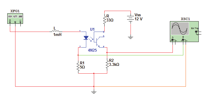
3. Single chaotic optocoupling device
3.1 Description of the circuit
There is a growing interest for non-autonomous chaotic signal generation circuits. Such a
circuit may be externally driven and it can typically consist of only one active and a few
passive components. Here, we consider a particularly simple circuit based on a single
optocoupling device. Its complete layout is shown in figure 9 and it consists of a 4N25
optocoupler, in a typical common emitter configuration, along with an emitter degeneration
resistor R2=3.3KΩ, a collector resistor R=33Ω, and a DC power supply VSS=12V. The circuit
is driven by an input sinusoidal voltage υIN(t) with amplitude Vin=13V and frequency f=800
Hz, which is applied through an inductor L=1mH connected in series to the driver LED and
a resistor R1, the value of which, as we will see, plays a crucial role in the circuit’s operation
and the generation of chaotic voltage time series across R1 and R2. In this respect, we use the
MultiSim circuit simulation software in order to examine the complete circuit operation by
monitoring the voltages υD(t) and υE(t) across R1 and R2, respectively.
Fig. 9. The optocoupling circuit and its MultiSim simulation environment
Optoelectronic Chaotic Circuits
639
Here, we must note that the considered circuit layout resembles the resistor-inductor-diode
(RLD) and the resistor-inductor-transistor (RLT) circuits, whose chaotic operation details
have been presented and discussed in (Hanias & Tombras, 2009). More specifically,
following the conclusions derived in (Hanias & Tombras, 2009), we use various values for R1
in order to achieve chaotic operation in both, if it is possible, the input LED loop and the
emitter output loop, i.e. across R1 and R2, respectively. Then, as mentioned above, the
simulated circuit operation is monitored by checking the voltages υD(t), across R1, and υE(t), across R2, since both of these voltage signals depend on the chosen value of the LED resistor
RD.
3.2 Simulation results
For the considered circuit operation simulation, we use υIN(t)= Vin sin(2π ft) with Vin=13 Volts and f=800 Hz. It is known that, chaotic operation may be generated under various operation
conditions and parameters’ values. In this chapter, we choose to keep Vin and f constant,
while varying the value of R1. Our goal is to first examine whether chaos can be achieve for
a specific R1 value and then to examine whether variation of that value of R1 may
strengthen, weaken, or even destroy the achieved chaos, by returning the circuit to its
typically expected operation.
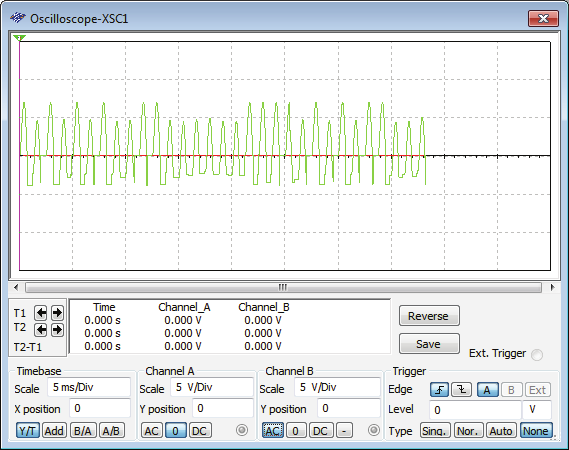
Under these conditions and after some try-and-error selections for the value of R1, we
conclude that if R1 is set equal to 5Ω then the circuit will exhibit a fully chaotic operation,
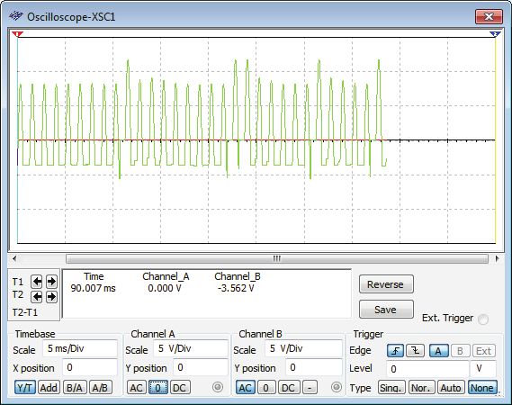
meaning that both voltage signals υD(t) across R1, and υΕ(t) across R2, are chaotic. This is readily shown in figure 10. Then, using this as starting point, we see that an increase of R1
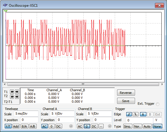
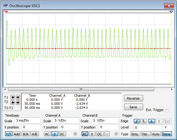
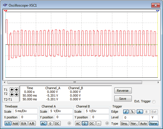
weakens the already obtained chaotic signals and this continues up to a value of R1=500Ω,
for which a weak chaotic signal can still be seen across R1, but not across R2. This is shown in
figure 11. Finally, further increase of R1 leads to the total destruction of the remaining
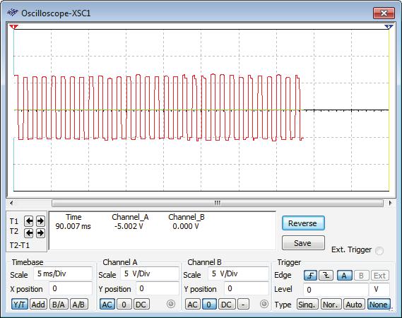
chaotic signal across R1. This is shown in figure 12 where, for R1=1KΩ, both voltage signals
υD(t) and υE(t) are not chaotic.
(a)
(b)
Fig. 10. For R1=5Ω: both voltage signals, (a) υD(t) across R1 and (b) υE(t) across R2, are chaotic
640
Optoelectronic Devices and Properties
(a)
(b)
Fig. 11. For R1=500Ω, (a) υD(t) is a weak chaotic signal across R1 and (b) υE(t), across R2, is non chaotic
(a)
(b)
Fig. 12. For R1=1KΩ, both voltage signals (a) υD(t) across R1 and (b) υE(t) across R2, are non chaotic
3.3 Nonlinear analysis
In this section, we proceed to the analysis of the obtained chaotic signals time series when
G
R1=5Ω. Using our data, with value of R1=5Ω we construct a vector X , i=1..N, where N=5000
i
data values in the m dimensional phase space given in the following form:
Optoelectronic Chaotic Circuits
641
G
X =
(5)
i
{υ υ, υ
i
, i , υ
…
ι
τ
−
− τ
2
i− m−1 τ }
(
)
This vector, represents a point of the m dimensional phase space in which the attractor is
embedded each time, where τ is the time delay τ=i Δt and Δt=0.1μs is the sample rate. The element υi represents a value of the examined scalar time series in time, i.e. here a voltage
value υ*, across R1 or R2, corresponds to the i-th component of the time series. The use of this method reduces phase space reconstruction to a problem of proper determination of suitable
values of m and τ. The choice of these values is not always simple, especially when there is
no additional information about the original system and the only source of data is a simple
sequence of scalar values as acquired from that system.
The dimension, where a time delay reconstruction of the phase space provides for the
necessary number of coordinates to unfold the dynamics from overlaps on itself caused by
projection is called embedding dimension m. Using the average mutual information, we can
then obtain τ as being less associated with a linear point of view, and thus, more suitable for
dealing with nonlinear problems. The average mutual information I(τ), expresses the
amount of information (in bits), which may be extracted from the value in time υi about the
value in time υi+τ. As optimum τ, suitable for the phase space reconstruction, the position of
the first minimum of I(τ) is usually used. In this case τ =77 time steps for chaotic signal
across emitter resistor R2 and τ=38 steps for chaotic signal across LED resistor R1 as shown in figure 13.
3.0
3.0
2.5
2.5
2.0
2.0
τ)
τ)
I(
I(
1.5
1.5
1.0
1.0
0.5
0.5
0
20
40
60
80
100
0
20
40
60
80
100
τ
τ
(a)
(b)
Fig. 13. Mutual information I versus time delay τ for both chaotic signals across (a) R1=5Ω
and (b) R2
Next, we use the method of False Nearest Neighbors (FNN), [Hanias et al., 2010], in order to
estimate the minimum embedding dimension. This method is based on the fact that when
the embedding dimension is too small, the trajectory in the phase space will cross itself.
Hence, if we are in position to detect these crossings, we may decide whether the used m is
large enough for correct reconstruction of the original phase space [i.e. when no
intersections occur] or not. If, however, intersections are present for a given m, then the
embedding dimension must be considered too small and it must be increased by one at
least. Then, again, we test the eventual presence of self-crossings.
642
Optoelectronic Devices and Properties
The practical realization of the described method is based on testing the neighboring points
in the m-dimensional phase space. Typically, we take a certain amount of points in the phase
space and find the nearest neighbor to each of them. Then we compute distances for all
these pairs and also their distances in ( m+1)-dimensional phase space. The rate of these
distances is given by
G
X m
X
m
i (
G
+ 1) − n i
1
( ) (
+ )
P =
G
(6)
X m
X
m
i (
) G
− n( i) ( )
G
where X m represents the reconstructed vector as described in (1), belonging to the i-th
i (
)
point in the