5.6
2.6
coefficient / (10-6/ºC)
Dielectric constant
5.7 9.7 12.5 10.9 9
11.8
Resistivity/(Ω·cm) >1013 150 108 1011 >1010
105
Electron mobility
2200 400 8500 1350 1250
1500
/(cm2/V·s)
Hole mobility
1800 50 400 120 850
600
/(cm2/ V·s)
Breakdown
1000 400 40 0.15 >100
30
field/(104V/cm)
Thermal conductivity
20 5 0.46 1.3
1.5
/(W·cm-1·K-1)
Electron sacturated
2.7 2.5 1
2.2
1
velocity/(107cm/s)
Working temperature
<800 130 300 >300
77
/( ºC)
Table 1. Comparison of properties between diamond, GaN, SiC and commonly used
semiconductors
In this paper, high quality freestanding diamond (FSD) films and formation of H-terminated
p-type channel on the diamond film surface were investigated and the origin of this H-
terminated high-conductivity layer was discussed. The realization and properties of the
optically activated MESFETs were also described here.
2. Preparation and characterization of FSD films
In this work, a microwave plasma chemical vapour deposition (MPCVD) technique at 2.45
GHz using a gaseous mixture of methane, hydrogen was applied to deposit FSD films on p-
type low resistivity single crystalline silicon substrates. All three gases were metered into
the chamber using mass flow controllers. The deposition parameters for FSD films were
shown in table 2.
Flux of hydrogen
Flux of methane
Chamber pressure
Substrate
(sccm)
(sccm)
(KPa)
temperature (ºC)
100 1 4.5 800
Table 2. Parameters for FSD deposition
After deposition, the silicon substrates were chemically etched to obtain FSD films with a
smooth surface at the nucleation side. The FSD films were disposed in mixed solution of
H2O2 and H2SO4 for 15 min to eliminate non-diamond surface layer of the diamond films.
Thin-Film Diamond Phototransistors
75
These samples were then cleaned by ultrasonic vibration in deionized water. A thermal
annealing treatment in nitrogen atmosphere at 650°C for an hour was performed to further
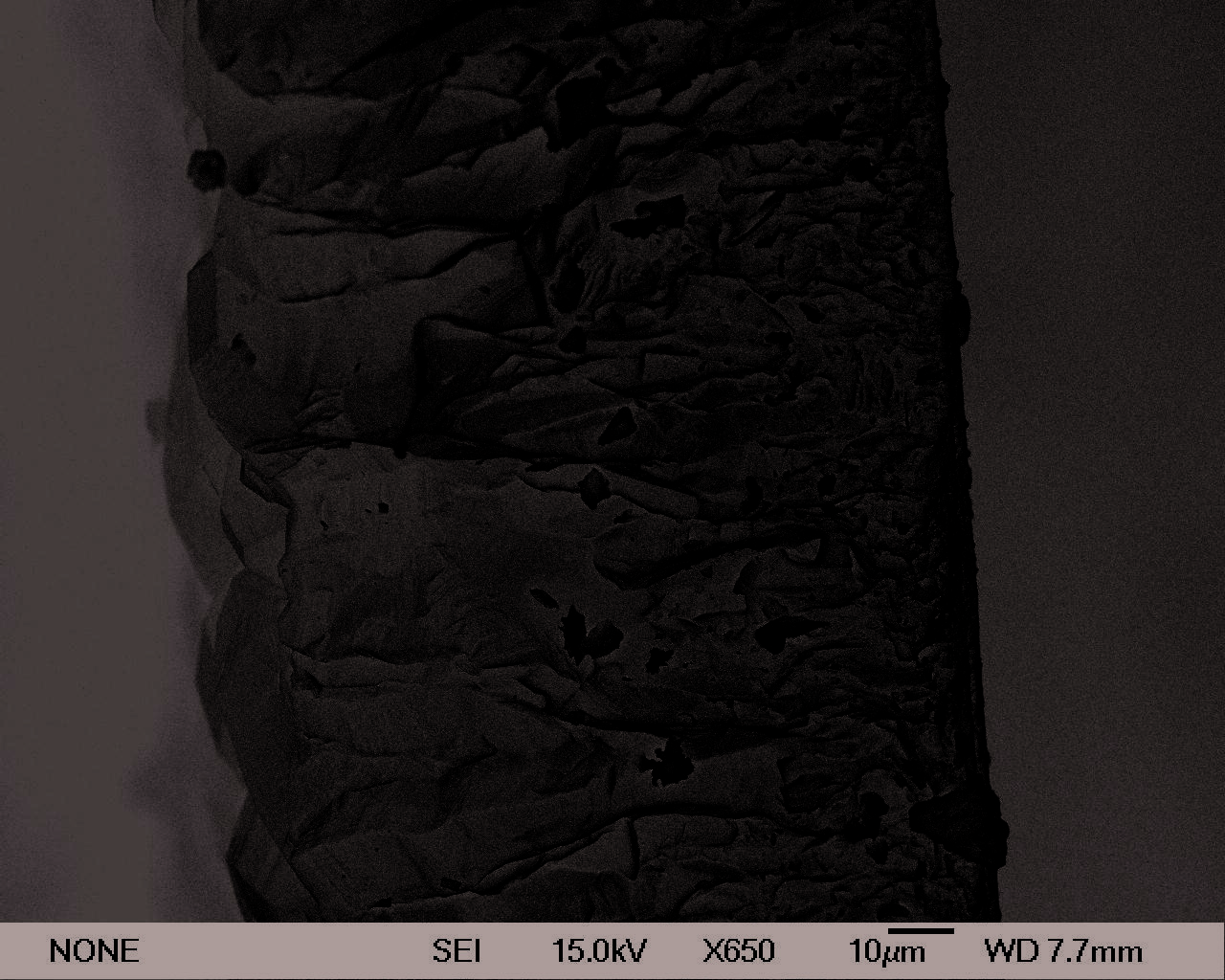
improve the quality of the diamond films. The thickness of the film was about 110μm, as
shown in Fig.1.
Fig. 1. Cross section image of the FSD film
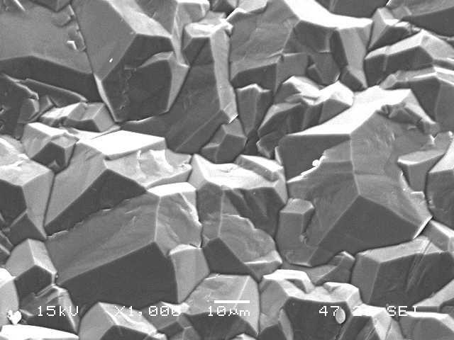
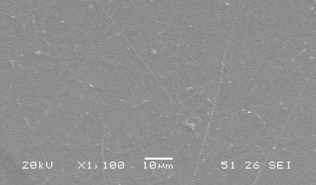
Figure 2 and figure 3 showed SEM images of growth surface and nucleation surface of FSD
films. The mean grain size of growth surface of the FSD film range from a few micrometers
to tens of micrometers and the growth surface was very rough. Whereas, the nucleation
surface was very smooth
Fig. 2. SEM image of growth surface of FSD
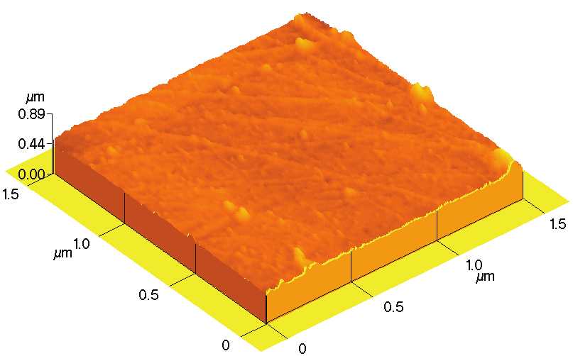
The typical AFM images of the nucleation side of FSD film are shown in Fig. 4, from which
it could be seen that the nucleation side was very smooth with a mean surface roughness of
about 10 nm in a scanning area of 1.5×1.5 μm2. The result was consistent with that obtained
from SEM images.
76
Optoelectronic Devices and Properties
Fig. 3. SEM image of nucleation surface of FSD
Fig. 4. AFM image of nucleation surface of FSD film
The Raman spectrum of the nucleation side of freestanding diamond film was shown in
Fig.5. For both FSD films with and without post-treatment, a strong Raman scattering peak,
located at about 1332cm-1, is the characteristic of diamond and a weaker Raman scattering
band, existed in range of 1400~1600cm-1, is the characteristic of non-diamond carbon [16]. It
is well known that the Raman signal for non-diamond carbon phase is about 75 times of that
for diamond. So Raman spectroscopy is also used to estimate the non-diamond carbon
content (Cnd) [17]: Cnd =1/ [1+75(Idia/Ind)], where Idia is Raman peak intensity for diamond
crystals and Ind is Raman peak intensity for non-diamond carbon phase. Therefore, the Raman
results from Fig.5 indicated a high quality diamond of nucleation side of FSD diamond films
with low content of non-diamond carbon. The Fig.5 also revealed that post-treatment (wet
chemical etch, annealing process) was helpful to improve the quality of FSD films.
Thin-Film Diamond Phototransistors
77
after treatment
1332cm-1
before treatment
.u.)
ity (ansteIn
1333cm-1
1200
1400
1600
Raman shift (cm-1)
Fig. 5. Raman spectrum of nucleation side of freestanding diamond film
3. Preparation and characterization of H-terminated p-type channel on FSD
films
The FSD films prepared above were exposed to hydrogen plasma at 750°C using a MPCVD
apparatus. The time of hydrogen plasma treatment on the p-type behavior of undoped FSD
nucleation surfaces were investigated by Hall Effect measurement. The electrical properties of
the FSD nucleation surfaces following different annealing temperature were also measured.
Figure 6 shows the sheet carrier density and sheet resistivity of p-type FSD films as a function of
time of hydrogen plasma treatment. The sheet carrier density rises with the time of hydrogen
plasma treatment and a stable value is achieved after about 30 min, whereas the sheet resistivity
reduces with time, with stable value being achieved after the same period of time.
The sheet carrier density and sheet resistivity of p-type FSD films as a function of annealing
temperature in air and in vacuum were shown in Fig.7 and Fig.8, respectively. All the FSD
films are exposed to hydrogen plasma treatment for 30 min at 750°C before a 180 min
annealing process. The values of sheet carrier density and sheet resistivity remained in a
relative stable range but change dramatically after annealing at temperature above 250 °C in
air, whereas the sheet carrier density and sheet resistivity kept a stable value up to 600°C in
vacuum.
Figure 9 and Fig.10 showed the values of sheet carrier density and sheet resistivity obtained
as a function of time that a sample had been annealed at various temperatures in air. The
data presented are typical of that obtained for many samples. Following annealing at 100 °C,
little variation was apparent in measurements taken over a prolonged period. However, if
the film was annealed at higher temperatures of 200 °C and 250°C the sheet carrier density
was seen to decrease with time, although a stable value was reached after a given period,
78
Optoelectronic Devices and Properties
whereas the film resistivity showed a reversed trend, gradually increasing to a stable
resistivity with the increase of annealing.
12
10
Sheet carrier density
Sheet resistivity
)
2
Sheet
/cm
8
12
10
resi
(10
st
6 ivity
8
r density
(10
rrie
4
4
Ω/cm
eet ca
2
)
6
Sh
2
5
10
15
20
25
30
Duration of hydrogen plasma treatment (min)
Fig. 6. Sheet carrier density and sheet resistivity of FSD against duration of hydrogen
plasma treatment
Sheet carrier density
Sheet resistivity
) 10
100
2 m
Sh
/c
eet
12
resi
1
(10
10
ty
stivity
0.1
r densi
1
(10
rrie
6
Ω
ca
/cm
0.01
0.1
2
)
Sheet
1E-3
0.01
0
50
100
150
200
250
300
Annealing te
mperature (oC)
Fig. 7. Sheet carrier density and sheet resistivity of FSD against annealing temperature in air
Thin-Film Diamond Phototransistors
79
15
0.3
Sheet carrier density
Sheet resistivity
)2m
Sheet
/c12 10
r
(10
0.2 esi
ty
stivity (
er densi
10
5
0.1
6
Ω/cm
2
)
Sheet carri
0
0.0
0
200
400
600
800
Annealing te
mperature (oC)
Fig. 8. Sheet carrier density and sheet resistivity of FSD against annealing temperature in
vacuum
14
)
2
12
/cm
12
10
(10
8
nsity
6
4
250oC
200oC
Sheet carrier de 2
100oC
0
50
100
150
200
250
300
Annealing time ( min)
Fig. 9. Sheet carrier density against time of annealing
It’s well known that the growth of diamond films at low pressure is a kinetic
nonequilibrium process because of the thermodynamic instability of diamond under these
conditions [18]. During such a nonequilibrium growth process, hydrogen plasma or atomic
80
Optoelectronic Devices and Properties
hydrogen radicals get rid of the graphitic phase, and sp3 species are rearranged to form
crystalline diamond by gradually adjusting their positions and orientations near the growth
face region [19]. The incompletely grown subsurface layer, where vacancies and dangling
bonds were concentrated, was continuously transformed into the ‘‘perfect’’ bulk diamond
[20]. Thus an imperfect thin layer will always exist on the diamond growth face. Hayashi et
al. also reported that high density hydrogen was incorporated into the subsurface region
rather than in bulk of as-grown diamond films by secondary ion mass spectroscopy (SIMS)
[21]. Therefore, the diamond surface conductivity may be related to the complexes of
absorbed hydrogen atoms with carbon dangling bonds. For example, if two adjacent carbon-
dangling bonds share one hydrogen atom, an acceptor state should be generated in the band
gap, since each hydrogen atom has only one electron.
0.25
250oC
2 ) 0.20
200oC
m
100oC
/cΩ6
10 0.15
(
vity sti 0.10
si
t ree 0.05
She
0.00
0
50
100
150
200
250
300
Annealing time ( min)
Fig. 10. Sheet resistivity against time of annealing
Starting from this point, the above experimental results can be well understood. The
nucleation surface of the CVD diamond film is full of defects (e.g., vacancies, dangling
bonds). The hydrogen plasma treatment may promote the complexes of hydrogen atoms
with vacancies and dangling bonds. After a period of time, a stable value of the sheet carrier
density is achieved when almost all the vacancies and dangling bonds are hydrogenated.
The sheet carrier density reduces after annealing at a temperature high enough, which is
due to desorption of hydrogen from the surface.
The loss of chemisorbed hydrogen from diamond surfaces requires temperatures of ~700 °C
to occur with any significant rate[22], so the simple loss of surface hydrogen would not
appear to account for the observations made here at temperature lower than 600°C in
vacuum. However, the loss of hydrogen from diamond could occur at temperatures lower
than 300 °C in air due to oxidation[23].
The fact that the sheet carrier density remains in the range of 1012 -1013 cm2 following a
annealing process below 250 °C in air and 600°C in vacuum suggests that the fabrication of
Thin-Film Diamond Phototransistors
81
devices which would operate up to this temperature using hydrogenation as a source of
carriers appears viable.
diamond
2d order
CHx
.u.)
nsity (a
Inte
(a)
(b)
2000
2500
3000
3500
4000
Raman shift ( cm-1)
Fig. 11. Ultraviolet Raman scattering spectra for hydrogenated diamond nucleation surface
sample (a) and annealed diamond surface sample (b)
2923
2851
2826
ance
(a)
Absorb
(b)
2600
2800
3000
3200
3400
Wavenumber (cm-1)
Fig. 12. Infrared spectra for hydrogenated diamond nucleation surface sample (a) and
annealed diamond surface sample (b)
82
Optoelectronic Devices and Properties
In order to take a further insight into surface conductivity of the nucleation surface of
diamond films, the ultraviolet Raman scattering spectroscopy was used to characterize
hydrogenated nucleation surface of diamond sample (a) and 500°C annealed (in air)
diamond surface sample (b). The magnified profiles of ultraviolet Raman scattering spectra
scanned in the 2000 -4000 cm−1 region were shown in Fig. 11. From the figure, sample (a)
and sample (b) both had a strong peak at about 2468.49 cm-1, representing the second order
of the diamond peak, and a weaker peak at about 2669.52 cm-1 and at 3148.26 cm-1,
representing the second order of the D band and G band of graphine respectively. However,
sample (a) had a stronger peak at 2930.93 cm-1 which indicates sp3 CHx [24], in comparison
with annealed nucleation surface of sample (b). It meant that, after annealed at a
temperature of 500 ºC in air, hydrogen desorbed from the nucleation surface of FSD films.
The internal reflection infrared spectrum obtained from sample (a) hydrogenated nucleation
surface of diamond and sample (b) 500°C annealed (in air) diamond surface were shown in
Fig. 6, from which the symmetric C-H stretching modes s at 2826 cm-1, symmetric stretching
mode of CH2 at 2851 cm-1 and the antisymmetric stretching mode of CH2 at 2923 cm-1 can be
observed in films after hydrogen plasma treatment[23,25]. However, there was no obvious
hydrocarbon adsorbates from the spectrum of Fig. 11(b) obtained after annealing at 500 °C
in air, which indicated that the hydrogen desorbed from the surface of diamond film after
annealing. All the above results confirmed that the diamond surface conductivity was
related to the complexes of absorbed hydrogen atoms with carbon dangling bonds.
4. Fabrication and characterization of phototransistor based on diamond
MESFETs
The FSD films were used to fabricate devices of MESFET. The fabrication of surface devices
using the nucleation surface of the FSD films solved the problem of the surface roughness
without the need of any kind of polishing. The smoothness of the nucleation surface allows
a higher control of the electrodes. And the problem of the high resistivity can be easily
overcome by a proper exposure of the surface to hydrogen plasma, as described above.
FSD films using for device fabrication were prepared as decribed in paragraph 2. Then, FSD
films were exposed to hydrogen plasma at 750°C for 30min using a MPCVD apparatus.
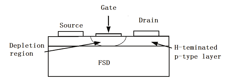
Fig. 13. A schematic the diamond MESFET device structure
Gold Ohmic contacts were evaporated as source (S), drain (D) and Aluminum contacts as
gate (G) by standard lithographic procedures. The thickness of the drain/source and gate

Thin-Film Diamond Phototransistors
83
contacts was 300nm and 200nm, respectively. The channel length and width were 10 μm
and 5 mm, respectively. The distance between Al electrode and Au electrode is about 10μm.
A schematic picture of the device structure and optical micrograph of the device were
shown in Fig. 12 and Fig.13, respectively. All devices were packaged and wire bonded prior
to testing.
Fig. 14. Optical micrograph of the MESFET device
Current-Voltage (I–V )behaviour of the gold-gold electrodes and aluminum-gold electrodes
on Hydrogen-teminated nucleation surface of FSD films were shown in Fig.14 (a) and Fig.14
(b). The I–V characteristics of adjacent Au contacts were near to linear, indicating Ohmic-
like behavior, however Al-Au electrodes showed a strongly asymmetric I-V behavior, due to
the presence of a Schottky barrier at the Al-diamond interface.
Figure 15 showed the Current-Voltage (I-V) behaviour of the source and drain electrodes
without any applied gate voltage. The gold electrodes, evaporated directly on the
Hydrogen-teminated nucleation surface of FSD films, behave as ohmic contacts. The small
asymmetry in the characteristics is related probably with a slight heating of the electrode
when the current starts to flow, increasing the resistivity of the material and producing an
extra decrease of the current [26].
Hydrogen-teminated FSD film MESFET structures, with an Al gate and Au source and drain
contacts, showed clear modulation of channel current as a gate bias was applied. The drain
current as a function of drain-source voltage (VDS) plotted for differing gate bias (VGS) was
shown in Fig.16. Field effect was seen for negative VGS, revealing a p-channel. There was no
current for VGS= 0 V, and channel current considerably increased as VGS was increased,
indicating the device was an enhancement-mode MESFET. For all gate bias values, IDS
saturated for higher VDS, indicating channel pinch-off.
Figure17 showed IDS against VDS with gate voltages of -0.1V which was illuminated with 200
nm light with varying intensity. The effect of the light is clearly to enhance the channel
current level, with increasing optical powers giving higher saturated IDS values. The results
suggest that phototrasistors based on hydrogenated diamond MESFETs may be ideally
suited for UV switching applications. The devices are not ‘‘visible blind’’ in the way that
photoconductive structures can be, but they do offer the potential of high switching speed
allied to high sensitivity.
84
Optoelectronic Devices and Properties
(a)
μA)
5
ent (
Curr
0
-10
-5
0
5
10
Voltage (V)
-5
7.5
(b)
5.0
Α)m 2.5
ent (
Curr
0.0
-2.5
-4
-2
0
2
4
Voltage (V)
Fig. 15. Current-Voltage behaviour of the gold-gold electrodes (a) and aluminum-gold
electrodes (b)
A PTI optical system and monochromator combination was used to investigate the response
of the device across the spectral range 200–350 nm. Responsivity of diamond
phototransistors as a function of illuminating wavelength with VDS of -12V was shown in
Fig.18. For the phototransistor, a pronounced increase in responsivity could be seen at
around 230 nm, which corresponds to the band-gap energy of diamond. The response at the
longer wavelengths (>300nm) was much smaller.
Thin-Film Diamond Phototransistors
85
1.0
0.5
0.0
(μA)
I DS
-0.5
-1.0
-10
-5
0
5
10
VDS(V)
Fig. 16. Current-Voltage behaviour of the source and drain electrodes without any applied
gate voltage
VGS
0
0.0V
-0.5V
μA) -20
(
DSt Ien -1.0V
rr -40
Cu
-1.5V
-60
-14
-12
-10
-8
-6
-4
-2
0
Voltage V (V)
DS
Fig. 17. Output characteristics of Hydrogen-teminated FSD film MESFET structures for
negative bias. Drain–source voltage (VDS) swept between 0 and -12 V; gate voltages (VGS)
swept between 0 and -1.5 V
86
Optoelectronic Devices and Properties
0