"This module was developed as part of a Rice University Class called "Nanotechnology: Content and Context"initially funded by the National Science Foundation under Grant No. EEC-0407237. It was conceived, researched, written and edited by students in the Fall 2005 version of the class, and reviewed by participating professors."
The semiconductor industry is one of the fastest growing manufacturing sectors in not only the United States but also in the world. According to the American Electronics Association, the domestic sales of electronic components have skyrocketed, jumping from $127 billion to $306 billion over the course of the 1980’s. In the first three quarters of the 2003 fiscal year alone, the export of technology goods from the United States increased by $19 billion [1].
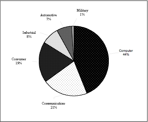
The word “semiconductor” technically refers to any member of a class of solid, crystalline materials that is characterized by an electrical conductivity better than that of insulators (e.g., plastic) but less than that of good conductors (e.g., copper) [2]. Semiconductors are particularly useful as a base material in the manufacturing of computer chips, and the term semiconductor has actually come to be synonymous with the computer chips, themselves. However, semiconductors are not only used in computers. Computers only make up 44% of entire industry consumption (see Figure 3.1). Semiconductors are also used for military, automotive, industrial, communications, and other consumer purposes.
Semiconductors seem to be anywhere and everywhere throughout our everyday lives, yet it is surprising how little most people know about how they actually work or about the potentially devastating effects their manufacturing can have on the environment and human health.
Much of the study of nanotechnology has been centered on the manufacturing of semiconductors. Though there are a number of highly anticipated applications for nanotechnology in other fields, notably in medicine and in biotechnology, the most tangible results thus far can be argued to have been achieved in the semiconductor industry.
For example, Intel recently unveiled its first products based on a generation of 90-nanometer process technology, and its researches and engineers have built and tested prototype transistors all the way down to the 22-nanometer range. Currently, Intel scientists and engineers are working on identifying new materials such as carbon nanotubes and nanowires to replace current transistors, and in particular they hope to develop a “tri-gate” transistor approach that would enable chip designers to build transistors below the 22-nanometer range [4].
With the advent of nanotechnology, these transistors are becoming even faster and more powerful, and in accordance with the law of accelerating returns, the industry has been producing smaller transistors at lower costs with each and every passing year. As these semiconductors become smaller and smaller, they are quickly and surely pushing towards the limits of the nano-realm.
These innovations, however, do not come without their fair share of challenges. Physical issues that are not problematic at the micron scale arise at the nano-scale due to the emergence of quantum effects, and in much the same way that optical microscopy cannot be utilized at the nano-scale, the semiconductor industry is fast approaching a similar diffraction limit. Optical lithography, for instance, a process that uses the properties of light to etch transistors onto wafers of silicon, will soon reach its limit.
At its most basic level, nanotechnology involves pushing individual atoms together one by one. Since approximately 1.7 billion transistors are required for a single chip, this is obviously not a realistic method for mass production. Unless an alternative method for production or a solution to this problem is found, the development and manufacturing of transistors are expected to hit a proverbial brick wall by the year 2015. This is the reason that research in nanotechnology is so important for the world and future of semiconductors.
Today’s semiconductors are usually composed of silicon, and they are manufactured in a procedure that combines the familiar with the bizarre; some steps that are involved in the process are as everyday as developing a roll of photographic film while others seem as if they would be better suited to take place on a spaceship.
These semiconductors appear to the naked eye as being small and flat, but they are actually three-dimensional “sandwiches” that are ten to twenty layers thick. It can take more than two dozen steps and up to two full months to produce a single one of these silicon sandwiches. Some of the basic and more essential steps involved in the manufacturing process of silicon chips are briefly detailed below.
First, silicon crystals are melted in a vat and purified to 99.9999% purity. The molten silicon is drawn into long, heavy, cylindrical ingots, which are then cut into thin slices called wafersabout the thickness of a business card.
One side of each wafer must be polished absolutely smooth. This process is called chemical-mechanical polishing, and it involves bathing the wafers in special abrasive chemicals. After chemical-mechanical polishing, imperfections cannot be detected on the wafers even with the aid of a laboratory microscope.
After a wafer is polished, layers of material must be stacked on top of the silicon wafer base. Insulating layers are laid down in alternation with conducting layers in a process called deposition. This is often achieved by spraying the chemicals directly onto the surface of the wafer through chemical vapor deposition. Following deposition, the wafer is coated with another layer of chemicals called a photoresist that is sensitive to light.
Next, a machine called a stepper (Figure 3.3) is calibrated to project an extremely fine and focused image through a special type of reticle film in a manner similar to that of a simple slide projector. The light that is transmitted through the reticle is projected onto the photoresist layer, which reacts to the light and begins to harden. All of the parts of the wafer exposed to this light harden into a tough crust while the parts in shadow remain soft. This particular step is known by the name of photoelectrochemical etching because it achieves an etching effect, resulting in a chip.
Hundreds of copies of the chip are etched onto the wafer until the entire surface has been exposed. Once this process is complete, the entire wafer is submerged into an etching bath, which washes away any parts of the photoresist that remain unexposed along with the insulating chemicals underneath. The hardened areas of the photoresist, however, remain and protect the layers of material underneath them. This process of depositing chemicals, coating with a photoresist, exposure to light over a film mask, and etching and washing away is repeated more than a dozen times. The result is an elaborate, three-dimensional construction of interlocking silicon wires.
This product is then coated with another insulating layer and is plated with a thin layer of metal, usually either aluminum or copper. Yet another photoresist is laid down on top of this metal plating, and after the wafer is exposed in a stepper, the process repeats with another layer of metal. After this step has been repeated several more times, a final wash step is performed, and a finished semiconductor product rolls off the assembly line, at last.
A typical semiconductor fabrication facility, or “fab” in industry jargon, looks like a normal two- or three-story office building from the outside, and most of the interior space is devoted to one or more “clean rooms,” in which the semiconductors are actually made. A clean room is designed with a fanatical attention to detail aimed towards keeping the room immaculate and dust-free (Figure 3.4).
Most if not all surfaces inside these clean rooms are composed of stainless steel, and these surfaces are sloped whenever possible or perforated by grating to avoid giving dust a place to settle. The air is filtered through both the ceiling and the floor to remove particles that are down to 1/100 the width of a human hair. Lighting is characteristically bright and slightly yellowish to prevent mildew from forming behind equipment or in recessed corners, and even the workers in a clean room must be absolutely spotless.
Workers in these rooms must be covered from head to toe in “bunny suits” that completely seal the body in a bulky suit, helmet, battery pack, gloves, and boots. Once sealed in these suits, the workers often look more like space explorers in a science fiction movie than computer chip employees, but in order to even enter the stainless steel locker room to suit up to begin with, they must first pass through a series of air lock doors, stand under a number of “air showers” that actually blow dust off of clothing, and walk across a sticky floor matting that removes grime from the bottom of shoes.
Semiconductor-manufacturing companies often portray their fabrication facilities as being clean, environmentally friendly, and conspicuously free of the black, billowing smokestacks that have come to be associated with the plants and factories of other major industries. These facilities produce no visible pollution and certainly do not appear to pose any health or environmental risks.
In truth, the term “clean room,” itself is more than just a bit of an understatement. Industry executives often boast that their clean rooms are from 1,000 times to 10,000 times cleaner and more sanitary than any hospital operating room.
The use of sterile techniques and the fastidious attention devoted to cleanliness in the semiconductor industry may perpetuate the illusion that the manufacturing of semiconductors is a safe and sterile process. However, as a rapidly growing body of evidence continues to suggest, hardly anything could be further from the truth (Figure 3.5). The question of worker safety and chemical contamination at chip-making plants has received an increasing amount of attention over the course of the past decade.
The devices being built at semiconductor fabrication facilities are super-sensitive to environmental contaminants. Because each chip takes dozens of trained personnel several weeks to complete, an enormous amount of time and effort is expended to produce a single wafer. The industry may pride itself on its perfectly immaculate laboratories and its bunny-suited workers, but it should be noted that the bunny suits are not designed to protect their wearers from hazardous materials but rather to protect the actual semiconductor products from coming into contact with dirt, hair, flakes of skin, and other contaminants that can be shed from human bodies. They protect the silicon wafers from the people, not the people from the chemicals.
Lee Neal, the head of safety, health, and environmental affairs for the Semiconductor Industry Association, has been quoted as saying, “This is an environment that is cleaner than an operating room at a hospital.” However, this boast is currently being challenged by industry workers, government scientists, and occupational-health experts across the country and worldwide.
Industrial hygiene has always been an issue in the semiconductor industry. Many of the chemicals involved in the manufacturing process of semiconductors are known human carcinogens or pose some other serious health risk if not contained properly. Table 3.1 lists ten of the hazardous chemicals most commonly used in manufacturing semiconductors along with their known effects on human health.
| Chemical name | Role in manufacturing process | Health problems linked to exposure |
| Acetone | Chemical-mechanical polishing of silicon wafers | Nose, throat, lung, and eye irritation, damage to the skin, confusion, unconsciousness, possible coma |
| Arsenic | Increases conductivity of semiconductor material | Nausea, delirium, vomiting, dyspepsia, diarrhea, decrease in erythrocyte and leukocyte production, abnormal heart rhythm, blood vessel damage, extensive tissue damage to nerves, stomach, intestine, and skin, known human carcinogen for lung cancer |
| Arsine | Chemical vapor deposition | Headache, malaise, weakness, vertigo, dyspnea, nausea, abdominal and back pain, jaundice, peripheral neuropathy, anemia |
| Benzene | Photoelectrochemical etching | Damage to bone marrow, anemia, excessive bleeding, immune system effects, increased chance of infection, reproductive effects, known human carcinogen for leukemia |
| Cadmium | Creates “holes” in silicon lattice to create effect of positive charge | Damage to lungs, renal dysfunction, immediate hepatic injury, bone defects, hypertension, reproductive toxicity, teratogenicity, known human carcinogen for lung and prostate cancer |
| Hydrochloric acid | Photoelectrochemical etching | Highly corrosive, severe eye and skin burns, conjunctivitis, dermatitis, respiratory irritation |
| Lead | Electroplated soldering | Damage to renal, reproductive, and immune systems, spontaneous abortion, premature birth, low birth weight, learning deficits in children, anemia, memory effects, dementia, decreased reaction time, decreased mental ability |
| Methyl chloroform | Washing | Headache, central nervous system depression, poor equilibrium, eye, nose, throat, and skin irritation, cardiac arrhythmia |
| Toluene | Chemical vapor deposition | Weakness, confusion, memory loss, nausea, permanent damage to brain, speech, vision, and hearing problems, loss of muscle control, poor balance, neurological problems and retardation of growth in children, suspected human carcinogen for lung and liver cancer |
| Trichloroethylene | Washing | Irritation of skin, eyes, and respiratory tract, dizziness, drowsiness, speech and hearing impairment, kidney disease, blood disorders, stroke, diabetes, suspected human carcinogen for renal cancer |
Several semiconductor manufacturers including National Semiconductor and IBM have been cited in the past for holes in their safety procedures and have been ordered to tighten their handling of carcinogenic and toxic materials.
In 1996, 117 former employees of IBM and the families of 11 workers who had died of cancer filed suit against the chemical manufacturers Eastman Kodak Company, Union Carbide Corporation, J. T. Baker, and KTI Chemicals, claiming that they had suffered adverse health effects as a result of exposure to hazardous chemicals on the job in the semiconductor industry [5]. The lawsuit was filed in New York, which prevented the employees from suing IBM directly. A separate group of former IBM workers who had developed cancer filed suit against the company in California, alleging that they had been exposed to unhealthy doses of carcinogenic chemicals over the past three decades. Witnesses who testified in depositions in the New York state court in Westchester County described how monitors that were supposed to warn workers of toxic leaks often did not function because of corrosion from acids and water. They also alleged that supervisors sometimes shut down monitors to maintain production rates. When they lodged complaints with senior officials in the company, they claim to have been told not to “make waves” [6]. Meanwhile, 70 female workers in Scotland sued National Semiconductor Corporation, another U.S.-based company, claiming that they, too, were exposed to carcinogens on the job.
These lawsuits and the resulting publicity prompted a groundbreaking study by the Health and Safety Executive, which commissioned a committee to investigate these allegations [7]. The committee found that there were indeed unusually high levels of breast and other kinds of cancer among workers at National Semiconductor’s fabrication facility in Greenock, Scotland. The committee concluded that the company had failed to ensure that the local exhaust ventilation systems adequately controlled the potential exposure of employees to hydrofluoric acid and sulphuric acid fumes and to arsenic dust. These findings proved to be extremely embarrassing for the company and for the industry. According to an official statement released by Ira Leighton, acting regional administrator of the New England branch of the U.S. Environmental Protection Agency, “National Semiconductor is a big business that uses a large amount of harmful chemicals and other materials. Our hazardous waste regulations were created to properly monitor dangerous chemicals and prevent spills. In order for it to work, it is important businesses to comply with all of the regulations. When companies fail to do this they are potentially putting people – their employees and neighbors – at risk [8]. ”
Moreover, a study of fifteen semiconductor manufacturers published in the December 1995 issue of the American Journal of Independent Medicine showed that women working in the so-called clean rooms of the semiconductor fabs suffered from a 14% miscarriage rate.

The main problem in prosecution is that the industry does not have a single overarching and definitive process for manufacturing, and it is difficult to pinpoint one particular compound as causing a certain health problem because some plants use as many as 300 chemicals. Also, many of the manufacturing processes take place in closed systems, so exposure to harmful substances is often difficult to detect unless monitored on a daily basis.
Executives and spokespeople for the semiconductor industry maintain that any chip workers’ cancers and other medical problems are more likely due to factors unrelated to the job, such as family history, drinking, smoking, or eating habits. They also say that over the years, as awareness of chemical hazards has grown, they have made efforts to phase out toxic chemicals and to lower exposure to others. They insist that they use state-of-the-art process equipment and chemical transfer systems that limit or prevent physical exposure to chemicals and point out that the substances used in the semiconductor industry are used in other industries without a major health or safety problem.
In theory, attention to cleanliness is in the manufacturer’s best interest not only from a health perspective but also from an economic. Many chemicals used in the production process are not expensive in and of themselves; however, the cost of maintaining these materials in an ultra-clean state can be quite high. This encourages the close monitoring of usage, the minimization of consumption, and the development of recycling and reprocessing techniques. Also, the rising costs of chemical disposal are prompting companies to conduct research into alternatives that use more environmentally friendly methods and materials. Individual companies and worldwide trade associations were active in reducing the use and emission of greenhouse gases during the 1990’s, and the industry as a whole has substantially reduced emissions over the last twenty years.
Nonetheless, there has been a history of environmental problems linked to the industry in Silicon Valley and other technology centers. To begin with, a tremendous amount of raw materials is invested in the manufacturing of semiconductors every year.
Moreover, a typical facility producing semiconductors on six-inch wafers reportedly uses not only 240,000 kilowatt hours of electricity but also over 2 million gallons of water every day [9]. Newer facilities that produce eight-inch and twelve-inch wafers consume even more, with some estimates going as high as five million gallons of water daily. While recycling and reusing of water does occur, extensive chemical treatment is required for remediation, and in dry or desert areas such as Albuquerque, New Mexico, home to plants for Motorola, Philips Semiconductor, Allied Signal and Signetics, Intel, and other high-tech firms, the high consumption of water necessary for the manufacturing of semiconductors can pose an especially significant drain on an already scarce natural resource [10]. The existence of economic mainstays including the mining industry and the established presences of Sandia National Laboratories and the Los Alamos National Laboratory make New Mexico an attractive location for high-tech tenants. However, the opening of fabrication facilities in the state leaves its farmers and ranchers in constant competition with the corporations for rights to water consumption. On average, the manufacturing of just 1/8-inch of a silicon wafer requires about 3,787 gallons of wastewater, not to mention 27 pounds of chemicals and 29 cubic feet of hazardous gases [11].