obtained from decomposing metalorganic precursors and reacting with oxygen.
Liewhiran et al [70] fabricated ZnO QDs with a diameter of 10-20nm which presented high
performance in ethanol sensors. Against aggregation, reducing the precursor feed rate helps
to decrease the diameter of ZnO QDs [68].
5. Vapor phase transport (VPT) deposition
The vapor phase transport (VPT) deposition process which needs very simple equipment
has been extremely wide and successful used in fabricating nano-sized compound materials,
including CdS, ZnS, ZnO, etc. [120-124]. The only equipment used in VPT process is a
horizontal tube furnace with high-temperature capacity. ZnO nanomaterials have obtained
great development via introducing this promising technique. The typical structures, such
nanowires, nanorods or array of nanorods and nanobelts, have been realized in the past
decade [122, 125-128]. 0D ZnO nanomaterials have been rarely reported until recently, Lu et
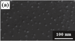
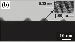
al [71, 72] reported fabrication of ZnO QDs with controllable size using VPT process. Figure
8 shows as-prepared ZnO QDs with a diameter around 7nm [71].


Synthesis, Self-assembly and Optoelectronic Properties
of Monodisperse ZnO Quantum Dots
225
In typical preparation, Znic acetate dihydrate (Zn(CH3COO)2·2H2O) was used as the zinc
source, while two gases, O2 and Ar, were input as oxygen source and carrier gas. A one-end-
sealed quartz tube was used to hold source materials and Si substrates. The whole quartz
tube was placed in a sealed horizontal tube furnace. High temperature was needed to
decompose metalorganic to vaporize metals and react with oxygen. ZnO QDs were
deposited at the low temperature zone where substrates were located.
Detailed study has been experimentally demonstrated that smaller size with better
dispersion of ZnO QDs could be achieved by reducing the growth time at the highest
temperature (Figure 8).
Fig. 8. (a) Plan-view and (b) cross-sectional TEM images of as-prepared ZnO QDs. An inset
high-resolution TEM image shows that the ZnO QDs are single crystal. (Courtesy of J. G. Lu
et al. [71])
5. Self-assembly of ordered 2D and 3D superlattices of ZnO QDs
ZnO is a luminescent, wide-band-gap semiconductor material that may find applications in
a wide range of domains. However, many applications require the organization of the
nanoparticles into two- or three-dimensional (2D or 3D) superlattices.[129] Recently, Bruno
Chaudret and co-workers reported a study concerning the conditions governing the
formation in solution and the dissolution of superlattices of ZnO QDs in the presence of
long-alkyl-chain amines, carboxylic acids, or binary amine/carboxylic acid mixtures.[130-
131]
The synthesis of ZnO QDs is carried out by slow hydrolysis in air of a THF solution
containing the precursor ZnCy2 as well as one equivalent of a long-alkyl-chain amine and
226
Optoelectronic Devices and Properties
half an equivalent of a long-alkyl-chain acid. Thus, when the reaction mixture was exposed
to air and left withstanding room temperature, the solvent slowly evaporated, left with
white and luminescent products. 2D organizations were spontaneously obtained by
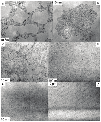
depositing one drop of the colloidal solution onto a carbon coated copper grid. Table 1
summarizes the results obtained under various reaction conditions and Figure 9 illustrates
some examples of the materials obtained.
Ligand[a] (per mole ZnCy2)
Solvent
Nanoparticle size [nm][b]
HDA/0.5 OcA
THF
3.5 ±1.0
HDA/0.5 OlA
THF
3.1 ±1.1
HDA/0.5 LcA
THF
2.8 ±0.8
DDA/0.5 OcA
THF
3.5 ±0.9
DDA/0.5 OlA
THF
3.5 ±1.7
DDA/0.5 LcA
THF
3.5 ±1.0
OA/0.5 OcA
THF
3.1±0.9
OA/0.5 OlA
THF
3.7±0.9
OA/0.5 LcA
THF
3.2±0.7
OA/0.5 OcA
3.6 ±1.1
OA/0.5 OlA
3.8 ±1.8
OA/0.5 LcA
3.7 ±1.4
2OA/0.5 OlA
3.6 ±1.4
5OA/0.5 OlA
3.4±1.5
Table 1. All procedures were carried out at room temperature, with an incubation time of 17
hours. The particles then were maintained in moist air for 4 days. For each experiment, the
concentration of the zinc precursor was 0.042 M. [a]: HDA, DDA, OA, OcA, OlA, and LcA
stand for hexadecylamine, dodecylamine, octylamine, octanoic acid, oleic acid, and lauric
acid, respectively. [b]: The mean diameter of the obtained nanoparticle was evaluated by
fitting of the histogram with a Gaussian curve. The first value corresponds to the centre of
the peak whereas the second one corresponds to two times the standard deviation of the
Gaussian distribution, or approximately 0.849 times the width of the peak at half height.
(Courtesy of M. L. Kahn et al. [130])

Synthesis, Self-assembly and Optoelectronic Properties
of Monodisperse ZnO Quantum Dots
227
Fig. 9. TEM pictures of ZnO nanoparticles obtained in the presence of: a) OA and OlA (1:1)
without other solvent; b) OA and OlA (2:1) without other solvent; c) OA and OlA (10:1)
without other solvent; d) OA and LcA (1:1) in THF; e) DDA and OcA (1:1) in THF; f) HDA
and OlA (1:1) in THF. (Courtesy of M. L. Kahn et al. [130])
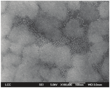
3D superlattices were obtained through slow evaporation of colloidal THF solutions. The
superlattices are not monodisperse in size but display uniform hexagonal shapes.
Interestingly, this shape may be related to the intrinsic hexagonal crystallographic structure
of ZnO, as previously observed for the organization of iron nanocubes.[132, 133] Figure 10
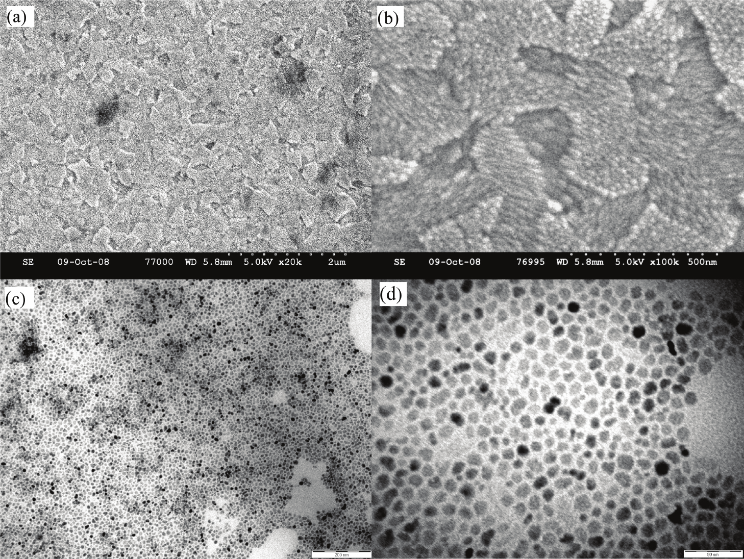
shows SEM image of small 3D superlattices of 3.1 nm ZnO nanoparticles obtained from
HDA and OlA. Larger 3D superlattices may be obtained when crystallization is performed
until the quasi-complete evaporation of the solvent.
In addition, Chen et al. [134] also reported that highly ordered, free-standing, complex, 2D
or 3D nanoparticle superlattice arrays were created by either evaporation-induced self-
assembly or precipitation-induced self-assembly from the size-monodispersed ZnO
nanoparticles functionalized by carboxylic and alkylthiol ligands recently. The synthesis of
the constituent ZnO nanoparticles is both novel and facile and is suggested as a generic
means of producing oxide nanomaterials by reaction of metal cations and oxide anions in


228
Optoelectronic Devices and Properties
alcohol solutions at room temperature. The regularity of the nanoparticle products and their
chemical functionalization provides the means to achieve superlattice thin films on indium
tin oxide (ITO)-coated glass slides (Figure 11).[134]
Fig. 10. SEM image of 3D superlattices of ZnO QDs prepared in the presence of HDA and
OlA. (Courtesy of M. L. Kahn et al. [130])
Fig. 11. EISA of OLA-ZnO QD superlattices. The (a) low- and (b) high-magnification SEM
images of the layered 3D OLA-ZnO NP superlattice film and the (c) low- and (d) high-
magnification TEM images of the 2D OLA-ZnO NP superlattice array self-organized on ITO
slides. (Courtesy of L. Chen et al. [134])
Synthesis, Self-assembly and Optoelectronic Properties
of Monodisperse ZnO Quantum Dots
229
The functionalization of these ZnO nanoparticles by long-chain carboxylic acids or
alkylthiols improves the size monodispersivity, and semiconduction properties
dramatically. The 2D or 3D self-assembly process is driven by the interfacial energy
minimization between polar solvents and the hydrophobic moieties of OLA-ZnO NPs
where well-organized, ordered nanoparticle superlattice structures are produced by either
evaporation-induced self-assembly (EISA) or precipitation-induced self-assembly (PISA).
6. ZnO QDs optoelectronic properties and application
1. The Photoluminescence and Bandgap of ZnO QDs
The photoluminescence (PL) spectrum of the as-prepared ZnO QDs sample reported by Hu
et al. [41], was measured at room-temperature with the excitation at a wavelength of 325
nm, as shown in Figure 12. A strong UV light emission peak is clearly observed at 362 nm,
corresponding to transition energy of 3.42 eV. A remarkable blue shift of 0.16 eV with
respect to the gap energy (3.26 eV) of bandedge emission of bulk ZnO crystals is obtained
due to the quantum confinement effect in ZnO QDs. [135] The corresponding band-gap
energy is larger than the emission peak energy by the excitonic binding energy. Such an
enlarged band gap implies a diameter of 3.5 nm of QDs.[136]
362
).u
nsity (ateIn
355
360
365
370
Wavelength(nm)
Fig. 12. PL spectrum of ZnO nanocrystals (λex=325nm). [41]
The ZnO nanodots were assembled into an ITO/ZnO/SiO2/Al structure (see Scheme 1) in
order to further determine the band alignment of ZnO nanodots on ITO via analysis of I-V
characteristics. Figure 13 presents the band diagrams of the ITO/ZnO/SiO2/Al structure
under the two opposite biases. Due to high barriers in both conduction and valence bands
at the Al/SiO2 interface, electron and hole injections from the SiO2 end were negligible. This
is evidenced by the experimental result that the current ratio of ITO/ZnO/SiO2/Al to
ITO/SiO2/Al is about 100. Figure 14a shows the forward biased I-V characteristics of these


![]()


