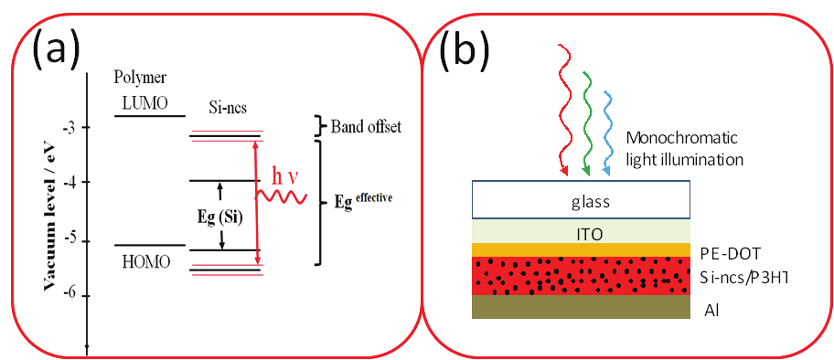
device based on Si-ncs prepared by laser ablation and electrochemical etching. Fig 7(b)
Hybrid Optoelectronic and Photovoltaic Materials based on
Silicon Nanocrystals and Conjugated Polymers
207
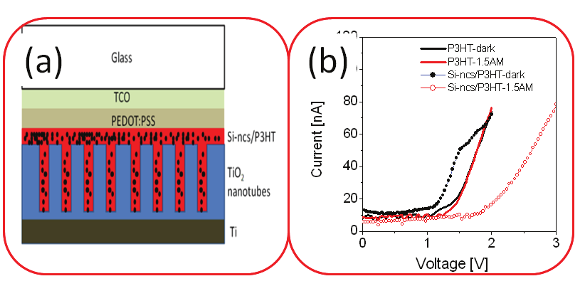
represents schematic structure of Si-ncs/P3HT blend based device. Glass substrate with an
ITO electrode was used and an alumina top electrode was deposited on top of Si-ncs/P3HT
active layer.
Fig. 7. (a) Energy band diagram of the MEH-PPV polymer and Si-ncs. (b) Schematic
structure of Si-ncs/polymer blend based device
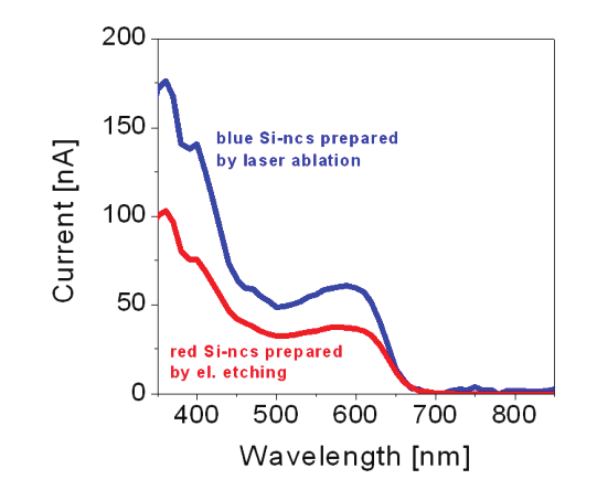
Fig. 8. Photocurrent generation in the Si-ncs/P3HT blends (~38 wt. % concentration of Si-
ncs) synthesized by two methods. Red line represents blend with the Si-ncs prepared by
electrochemical etching and the blue line by nanosecond laser ablation in water
208
Optoelectronic Devices and Properties
Figure 8 compares photocurrent generation as a function of the wavelength for blends
containing of the Si-ncs blended at ~ 38 wt. % concentration. Red line corresponds to the Si-
ncs prepared by electrochemical etching and blue line to Si-ncs synthesized by laser ablation
in water. A more important increase in photoconductivity is noticed for the films containing
of the blue-luminescent nanocrystals prepared by laser ablation. Similar to disccused above
(Švrček et al., 2009c), it is believed that large fraction of the excitons dissociates at Si-
nc/polymer interface. Since Si-ncs prepared by laser ablation are smaller in radius (1.5-3
nm) the bulk-heterojunction inteface for exciton dissociation is larger. Then the exciton
separation rate is superior to the blend fabricated from the electrochemically etched Si-ncs
where the radius is 3-5 nm in average.
6. Filtering and ordering of Si-ncs/co-polymers hybrid composites in
nanotubes
It is believed that arrangement of flexible Si-ncs based blends in a form of long nanofibers
could resolve multiple problems. It is supposed that the fibrous-like structure will lead to an
alignment of Si-nc polymer chains and allow the formation of thicker devices. The nanofiber
perpendicular orientation might improve charge collection efficiency through the creation of
uninterrupted percolation paths for photogenerated carriers generated by bulk-
heterojunction. Noteworthy to say that the nanofiber structure provides a larger interfacial
area and has a much lower reflectance compared with the thin films. Several nanotubular
architectures have been investigated for potential enhancement of electron percolation
pathways in bulk-heterojunction (Coakley et la.,2003). We believe that the nanoporous
anodic alumina and TiO2 are the most feasible large-scale templates that can be used for
blend alignment. Furthermore, the size distribution of freestanding Si-ncs can be improved
by filtering across the anodic alumina membrane (Švrček et al., 2010). The filtering through
the alumina membrane can be used to narrow the size distribution of Si-ncs blended with
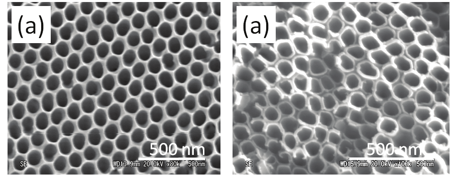
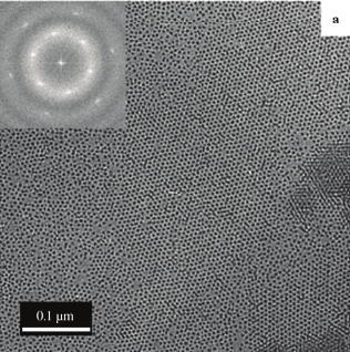
MEHPPV polymer as well. Figure 9 (a) presents typical top-view SEM images of the
nanoporous membrane with an average diameter of 85 nm. The SEM image shows a well-
ordered hexagonal packing of the alumina nanopores with a uniform pore size distribution.
The high surface energy and O-ring that seal the edges of the membrane kept the liquid on
the top of the alumina membrane within the O-ring (Švrček et al., 2010). Then, induced
capillary forces from the bottom establish the liquid flow through the opened alumina
membrane.
Wettability is another important factor, which contributes to the establishing the flow across
one membrane (Švrček et al., 2010). The Young–Laplace equation is commonly used to
describe the pressure drop across (Marle, 1981). Once the flow is established, the
hydrodynamic flow can be described by the Hagen–Poiseuille equation (Blom, et al., 1996,
Švrček et al., 2009c). In this case we deal with the large diameter of pores (Švrček et al.,
2010), the flow rate (R) across the alumina nanoporous membrane can be written as
4
π d ⎛ P ⎞
R =
(2)
128η ⎜ L ⎟
⎝ ⎠
where P is the pressure drop across the pore, d is the pore diameter, η is the solvent
viscosity, and L is the membrane thickness. It has to be noted that we achieved the capillary
induced wetting of the nanopores when the viscosity of the Si-ncs/MEH-PPV blend
Hybrid Optoelectronic and Photovoltaic Materials based on
Silicon Nanocrystals and Conjugated Polymers
209
dropped on top of nanoporous alumina was high enough to prevent free flow of the blend
through the membrane. Compared to TiO2 advantageous of alumina membrane is that it is
easily to be dissolved without dissolution of blend. After dissolution of the membrane in
weak 5 wt % phosphoric acid, we could observe the presence of a Si-ncs/MEH-PPV
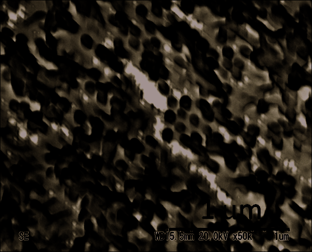
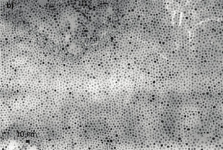
nanofibrous blend. Figure 10 shows typical SEM image of the Si-ncs/MEH-PPV nanofibers
after dissolution of the nanoporous alumina membrane. Our observation showed the
formation of randomly oriented long fibers only, without the presence of nanotubes. The
diameter of the fibers corresponds to the diameter of the alumina nanopores ~80 nm. The
wetting phenomena and the presence of Si-ncs in the polymer did not allow formation of
nanotubes. However, the nanoporous alumina membrane was quite thick 50 μm and the
perpendicularly ordered fibers collapsed. The EDS spectra reveal less oxygen in the blend
when after filtering (Švrček et al., 2010). It is supposed that an improvement of both the Si-
nc size distribution and the blend morphology limits the oxygen diffusion into the blend. It
is well known that oxygen is one of the main factors that lead to the degradation of
conjugated polymer-based devices (Scott, et al., 1996]). As this processing can be performed
at room temperature it might find application in the future development of new types of
optoelectronic and photovoltaic devices.
Fig. 9. (a) Top-view SEM images of the nanoporous membrane with average diameter of ~85
nm used for experiments. (b) SEM image of the nanotubular TiO2 template with diameter of
~90 nm used for vertical order of Si-ncs conjugated polymer based blend
Previous experiments confirmed that the blend can flow through pores with such a
diameter. Following of those experiments we have used TiO2 nanotube template with rather
same diameter that the same time serves as an electrode for hybrid device. The morphology
of the TiO2 nanotube with average diameters of 90 nm after thermal treatment is shown in
Fig. 9 (b). The transformation of amorphous TiO2 into crystalline anatase was confirmed by
XRD measurements and after the annealing process two most important TiO2 anatase peaks
corresponding to (101) and (200) orientations were clearly recorded (Švrček et al., 2009b). It
is observed that infiltration of photosensitive Si-ncs/P3HT blend in the TiO2 nanotubes
results in increase in the photovoltage generation. One can expected that the alignment of
Si-ncs/P3HT bulk-heterojunction within TiO2 nanotubes, which are perpendicular to the
contact, will facilitates charge transfer along the nanotubes and reduces losses incurred by
charge hopping across the Si-ncs/P3HT blend (Švrček et al., 2009b). Figure 11 (a) shows a
210
Optoelectronic Devices and Properties
Fig. 10. Scanning electron microscopy image of the Si-ncs/MEH-PPV nanofibers after
dissolution of the nanoporous alumina membrane
Fig. 11. (a) Schematic sketch of the structure for ordering of Si-ncs/P3HT bulk-
heterojunction in TiO2 nanotube arrays. (b) The current voltage (I–V) characteristics from the
pure P3HT polymer and Si-ncs/P3HT blend aligned in within TiO2 nanotube arrays with
the diameters of 90 nm in dark and under illumination AM1.5
schematic sketch of the structure used for alignment of Si-ncs/P3HT bulk heterojunction.
The corresponding I–V characteristics of Si-ncs/P3HT heterojunction in vertical
configuration in the dark and under illumination at AM1.5 are compared in Fig. 11 (b). The
I–V characteristics for P3HT polymer only and Si-nc/P3HT based blend show a p–i–n
behavior. However, superior open voltage and ratio between the photo- and dark-
Hybrid Optoelectronic and Photovoltaic Materials based on
Silicon Nanocrystals and Conjugated Polymers
211
conductivity are observed in the case of infiltration of the blend into TiO2 nanotubes
(symbols in Fig. 11 (b)). The photovoltage generation in the bulk-heterojunction most likely
results in increase in open circuit voltage. The presence of the Si-ncs in polymer makes the
blend to be more semiconductor rather than an insulator; therefore, a high-voltage open-
circuit can be partially explained by assuming a Schottky barrier at the Si-
ncs/P3HT/PEDOT:PSS interface. The fiber-like geometry provides larger interfacial area,
which results in enhanced exciton dissociation. The nanofiber morphology of the blend
embedded into nanotubular templates contributed to high open-circuit voltage.
7. Conclusion
We showed that electrochemical etching and nanosecond laser ablation in water are suitable
techniques for preparing freestanding and surfactant-free Si-ncs with quantum
confinements effects. It is demonstrated that such Si-ncs can be successfully used for the
fabrication of room temperature photoluminescent and photosensitive hybrid materials. The
materials consisting of Si-ncs with rather different energy band gaps and conjugated
polymers (poly(3-hexylthiophene) (P3HT) and poly(methoxy ethylexyloxy
phenylenevinilene) (MEH PPV)) with rather similar energy band gaps were fabricated. We
argue that the luminescence and transport properties of the blends can be controlled by the
Si-ncs properties and could be assigned to quantum confinement of excitons in
nanocrystalites. The difference in electron affinity and ionization potential between
nanocrystals and polymer leads to bulk-heterojunction formation and excitons desociation.
An enhanced photovoltaic effect has been achieved by blending of Si-ncs prepared by laser
ablation. The device performances have been improved through enhanced bulk-
heterojunction interface area and charge transport. Next, we showed that the nanotube
arrays can be efficient for a vertical 1D-like order of photosensitive hybrid material. An
arrangement of the Si-ncs/P3HT bulk-heterojunction within ordered Al2O3/TiO2 nanotubes
prepared perpendicular to the contact has been shown. It is believed that the Si-ncs non-
toxicity, easy integration into well-established silicon technologies and polymer flexibility
might bring considerable benefit for hybrid optoelectronic and photovoltaic device
development. Needless to mention that the blend flexibility might allow easy and cost
effective design new types of nanostructures for enhancement device properties.
8. Acknowledgements
This study was also partially supported by Industrial Technology Research Grant Program
from the New Energy and Industrial Technology Development Organization (NEDO) of
Japan.
9. References
Canham, L. T. (1990), Silicon Quantum Wire Fabrication by Electrochemical and Chemical
Dissolution of Wafer, Appl. Phys. Lett. 57, pp.1046-1048.
Beard, M.C.; Knutsen, K.P.; Yu, P.; Luther, J.M.; Song, Q.; Metzger, W.K.; Ellingson, R.J.;
Nozik, A.J., (2007), Multiple Exciton Generation in Colloidal Silicon Nanocrystals ,
Nano Lett. 7 , pp. 2506-2512.
212
Optoelectronic Devices and Properties
Blom, P. W. M.; De Jong, M. J. M. ; Vleggaar, J. J. M. (1996), Electron and hole transport in
poly( p-phenylene vinylene) devices, Appl. Phys. Lett. , 68 pp.3308(1-3).
Chang, T. W. F.; Musikhin, S.; Bakueva, L.; Levina, L.; Hines, M.A.; Cyr, P.; Sargent, E.H.;
(2004), Efficient excitation transfer from polymer to nanocrystals, Appl. Phys. Lett.
84, pp. 4295-4298.
Coakley, K.M.; Liu, Y.X.; McGehee, M.D.; Frindell, K.L.; Stucky, G.D. (2003), Infiltrating
semiconducting polymers into self-assembled mesoporous titania films for
photovoltaic applications, Adv. Funct. Mater. 13, pp. 301-316 .
Dexter, D.L., (1953), A Theory of Sensitized Luminescence in Solids J. Chem. Phys. 21, pp.
836-851.
Förster,T., (1959), 10th Spiers Memorial Lecture. Transfer mechanisms of electronic
excitation Discuss. Farraday Soc. 27, pp. 7-17.
Garcia, C.; Garrido, B.; Pellegrino, P.; Ferre, R.; Moreno, J.A.; Morante, J. R.; Pavesi, L.;
Cazzanelli, M., (2003), Size dependence of lifetime and absorption cross section of
Si nanocrystals embedded in SiO2, Appl. Phys. Lett. 82, pp. 1595 -1598.
Greenham, N. ; Peng, X.; Alivisatos, P. (1996), Charge separation and transport in
conjugated-polymer/semiconductor-nanocrystal composites studied by
photoluminescence quenching and photoconductivity, Phys. Rev. B 54, pp. 17628-
17637.
Harris, P.F.J. (2002). Carbon nanotubes and related structures (1st ed.). Cambridge University
Press. pp. 213–32
Herman. F.; Kasowski, R. V., (1981), Electronic structure of defects at Si/SiO2 interfaces, J.
Vac. Sci. Technol. 19, pp. 395-401.
Hirsmman, K. D.; Tsybeskov, L.; Duttagupta, S. P.; Fauchet, P. M. , (1996), Silicon-based
visible light-emitting devices integrated into microelectronic circuits, Nature 384,
pp. 338-341.
Inzelt, G.; (2008). Conducting Polymers A New Era in Electrochemistry . Springer. pp. 265–269.
Iijima, S. (1991). Helical microtubules of graphitic carbon, Nature, 354, pp. 56-58.
Jurbergs, D.; Rogojina, E.; Mangolini, L.; Kortshagen, U., (2006), Silicon Nanocrystals with
Ensemble QuantumYields exceeding 60%, Appl. Phys. Lett. 88, pp.233116 -233119.
Kovalev, D. I.; Yaroshetzkii, I. D.; Muschik, T.; Petrovakoch, V. F.; Koch P., (1994), Fast and
slow visible luminescence bands of oxidized porous Si, Appl. Phys. Lett. 64, pp.214 -
217.
Lulease, J.; Fujii, M.; Mimura, A.; Hayashi, S., (2002) Phys. Rev. Lett. 89 pp.296805-.296809.
Liu, J.L.; Yan, B.; (2008), Molecular Construction and Photophysical Properties of
Luminescent Covalently Bonded Lanthanide Hybrid Materials Obtained by
Grafting Organic Ligands Containing 1,2,4-Triazole on Silica by Mercapto
Modification, J. Phys. Chem. C 112, pp. 14168-14178.
Lui, C., Holman, Z., Kortshagen, U., (2009), Hybrid Solar Cells from P3HT and Silicon
Nanocrystals , Nano Lett. 9, pp. 449-452.
Marle, C. M. (1981), Multiphase Flow in Porous Media, Gulf, Houston, TX .
Martel, R.; Derycke, V.; Lavoie, C.; Appenzeller, J.; Chan, K. K.; Tersoff, J.; Avouris, Ph.
(2001), Ambipolar Electrical Transport in Semiconducting Single-Wall Carbon
Nanotubes, Physical Review Letters 87: pp. 256805-256809.
Hybrid Optoelectronic and Photovoltaic Materials based on
Silicon Nanocrystals and Conjugated Polymers
213
Murray, C.B.; Kagan, C.R.; Bawendi, M. G. (2000), Synthesis and Characterization of
Monodisperse Nanocrystals and Close-Packed Nanocrystal Assemblies, Annual
Review of Materials Research 30 (1): pp. 545–610.
Ourmazd, A.; Taylor, D. W.; Rentschler, J.A.; Bevk, J. (1987), Si→SiO2 transformation:
Interfacial structure and mechanism," Phys. Rev. Lett. 59, pp. 213-216.
Scott, J. C. ; Kaufman, J. H. ; Brock, P. J. ; DiPietro, R. ; Salem, J.; Goitia, J. A.; (1996),
Degradation and failure of MEH-PPV light-emitting diodes, J. Appl. Phys. , 79, pp.
2745-2752.
Schneider, M.; Muller, K.,; (2000), Hybrid Materials Doped with Covalently Bound Perylene
Dyes through the Sol−Gel Process , Chem. Mater. 12 , pp. 352-362.
Sukhovatkin, V; Hinds, S.: Brzozowski, L.; Sargent, E.H.; (2009), Colloidal Quantum-Dot
Photodetectors Exploiting Multiexciton Generation, Science 324 pp. 1542-1544.
Švrček, V.; Pelant, I.; Chvojka, T.; Valenta, J.; Dian, J.; Rehspringer, J.-L.; Gilliot, P.;
Ohlmann, D.; Crégut, O.; Hönerlage, B., (2002), Photoluminescence properties of
sol-gel derived SiO2 films doped with porous silicon, Materials Science &
Engineering C 19, pp.233-238.
Švrček, V.; Slaoui, A.; Muller, J.-C. (2004), Ex-situ prepared Si nanocrystals: Their elaboration
and characterization in embedded silica glass, J. Appl. Phys. 95, pp.3158-3164.
Švrček, V. Sasaki, T.; Shimizu, Y.; Koshizaki, N., (2006), Blue luminescent silicon
nanocrystals prepared by ns pulsed laser ablation in water, Appl. Phys. Lett. , 89,
pp.213113(1-3).
Švrček, V.; Fujiwara, H.; Kondo M.; (2008a), Improved transport and photo-stability of
poly[methoxy-ethylexyloxy-phenylenevinilene] polymer thin films by boron doped
freestanding silicon nanocrystals, Appl. Phys. Lett. 92, p.143301(1-3).
Švrček, V.; Sasaki, T.; Shimizu, Y.; Koshizaki, N.; (2008b), Blue luminescent silicon
nanocrystals prepared by ns laser ablation and stabilized in electronically
compatible spin on glasses, J. Appl. Phys., 103, pp.023101-023108.
Švrček, V.; Mariotti, D.; Kondo, M.; (2009a), Ambient-stable blue luminescent silicon
nanocrystals prepared by nanosecond-pulsed laser ablation in water, Optics
Express, 17 pp. 520-527.
Švrček, V.; Turkevych, I.; Kondo, M.; (2009b) Photoelectric properties of silicon
nanocrystals/P3HT bulk-heterojunction ordered in titanium dioxide nanotube
arrays, Nanoscale Research Letters, 4 pp.1389-1395.
Švrček, V.; Fujiwara, H.; M. Kondo, M.; (2009c) Luminsecent Properties of doped
freestanding silicon nanocrystals embedded in MEH-PPV, Solar Energy Materials &
Solar Cells, 93, pp. 774-780.
Švrček, V.; Fujiwara, H.; Kondo, M.; (2009c) Top-down silicon nanocrystals and a conjugated
polymer-based bulk heterojunction : Optoelectronic and photovoltaic applications,
Acta Materialia 57 pp.5986-5997.
Švrček. V; Turkevych, K.; Kondo, M.; (2010) Filtering and assembly of Si
nanocrystals/conjugated polymers blend with reduced oxygen penetration, Journal
of the Electrochemical Society 157 (9) pp. K194-K200.
Tenne R, Margulis L, Genut M, Hodes G (1992), Polyhedral and cylindrical structures of
tungsten disulphide, Nature 360 (6403): pp. 444–446.
Yue, D.; Bai, X.; Zhao,S.; Miao,X.; Li, M.; Dong, J.; Ibrahim,K.; Wang, J.; Zhao,Y.; Yuan, H.;
Xing, G.; Sun, B.; (2010), First Endohedral Metallofullerene-Containing Polymer:
214
Optoelectronic Devices and Properties
Preparation and Characterization of Gd@C82-Polystyrene, The Journal of Physical
Chemistry C 114 (17), pp. 7631-7636.
Zhao, X.; Liu, Y.; Inoue, S.; Suzuki, T.; Jones, R. O.; Andol, Y. (2004), Smallest Carbon
Nanotube is 3 Å in Diameter, Physical Review Letters 92 (12) pp. 125502-125506.
Zhuravlev, K. S.; Gilinsky, A.M.; Kobitsky, A.Y., (1998), Mechanism of photoluminescence of
Si nanocrystals fabricated in a SiO2 matrix, Appl. Phys. Lett. 73, pp.2962-2965.
Wang, X.; Li, Q.; Xie, J.; Jin, Z.; Wang, J.; Li, Y.; Jiang, K.; Fan, S. (2009), Fabrication of
Ultralong and Electrically Uniform Single-Walled Carbon Nanotubes on Clean
Substrates, Nano Letters 9 (9): pp. 3137–3141
11
Synthesis, Self-assembly and Optoelectronic
Properties of Monodisperse ZnO Quantum Dots
Ting Mei1,2 and Yong Hu3
1Institute of Optoelectronic Materials and Technology, South China Normal University,
Guangzhou 510631,
2School of Electrical and Electronic Engineering,
Nanyang Technological University, 639798,
3Institute of Physical Chemistry, Zhejiang Normal University, Jinhua, 321004,
1,3China
2Singapore
1. Introduction
Quantum dot (QD), also called artificial atom, is a semiconductor nanocrystal with the size
on the order of a few nanometers. By modifying its composition, size and shape, its density
of electronic states can be engineered and thus many physical properties can be widely and
easily adjusted. Strong quantum confinement of electronic carriers at nanometer scale makes
band-gap and luminescence energies size and shape dependent. These dots have now been
widely employed as targeted fluorescent labels for biomedical applications.
Zinc oxide (ZnO) is a wide-band-gap semiconductor that presents interesting luminescent
properties, which are seen in the recent demonstration of ultraviolet lasing from nanowires.
These properties have stimulated the search for new synthetic methodologies for well-
controlled ZnO nanostructures. However, many applications require the organization of
nanoparticles into two- or three-dimensional (2D or 3D) superlattices. This very efficient
organization was obtained by physical methods, whereas chemical approaches toward such
organizations would also be of interest since they are easy to perform and allow a facile
scale-up procedure.
For the interest of size dependent physical properties, intensive research has been focused
on fabricating ZnO QDs with ultra small size that gives strong quantum confinement. By
far, various kinds of synthetic approaches have been realized in fabricating such small ZnO
QDs, which can be roughly divided into two categories, chemical and physical. Chemical
methods involves sol-gel method, hydrothermal growth, thermal decomposition,
electrochemical method, while physical methods involves pulsed laser ablation (PLA or
PLD), metalorganic chemical vapor deposition (MOCVD), radio frequency (RF) sputtering,
flame spray pyrolysis (FSP) method, vapor phase transport (VPT) deposition, etc.. Chemical
process takes advantage of the very exothermic reaction of the organometallic precursor
bis(cyclohexyl) zinc with water to produce crystalline zinc oxide on one hand, and on the
other hand the kinetic control of the decomposition by using long-alkyl-chain amine
ligands. However, if the use of amine ligands allows access to ZnO nanoparticles with low
size dispersity, these particles are not monodispersed, and consequently no 2D organization
216
Optoelectronic Devices and Properties
was observed. For metal-oxide nanoparticles, a few 2D organizations resulting from particle
self-assembly on a surface have been described. ZnO nanoparticles are produced by
evaporating the solvent of the reaction solution, a method used in molecular chemistry to
form monocrystals. In addition, the synthesis of Zn