procedure in this work are primarily dealing with a NbN superconducting nanowire, these
methods and procedures are applicable to other nano size optoelectronic devices, such as
high temperature superconducting or even semiconducting optoelectronic devices.
2. Equivalent circuit model for S-parameter measurement
2.1 The construction of the equivalent circuit model
We use the packaged SNSPD identical to what we have reported in (Yan et al., 2009)
to undertake all the measurements.
However, in the context of current chapter, NbN
nanowire meanderlines of the SNSPD are taken as the device under test (DUT). The nanowire
meanderline has the same geometrical sizes as what the SNSPD has. For DUT critical
temperature Tc, we use an alternative method to find its value. It is estimated to be close to 10.4
K, by the best fitting to the 1 − ( T/ Tc)4 like relation based on kinetic inductance-temperature
measurement. We will elaborate how to achieve the estimation in later sections. The exact
critical current density varies with different DUTs, but all are in the range above 106 A/ cm 2.
Since the measurement has to be performed in a packaged device, while the active area of
nanowire is relatively small, any distributed effect must be taken into account, including
geometrically induced magnetic inductance and capacitance, which are in addition to the
kinetic inductance Lk. The former most likely arises from interconnection wires; the latter
has been reported either originating from the stray capacitance (Yan et al., 2007; Semenov et
al., 2007), or from the dc bias circuitry (Yang et al., 2007). In addition, when the device is
dc biased, either with or without the presence of an RF signal, some resistance possibly due
to either phase slips or Joule heating may present along the nanowire (Tinkham et al., 2003).
We model such lossy contributions by a resistance term of Rs in series with Lk. Therefore,
the construction of an equivalent circuit model, which helps to exclude these unavoidable
elements, becomes the key to accurately measure Lk, under conditions of both current and
voltage bias schemes.
Fig. 1 shows the circuit model at both room and cryogenic temperatures. The procedures to
determine values of C, Lk and Rs are deduced from the model, provided that we know the
impedance Z 0 of transmission line, and room temperature resistance Rn (usually between 1.5
to 2 MΩ) of the NbN nanowire meanderline. The two-step procedure comprises room and
cryogenic temperature S-parameter measurements. Firstly, we perform a room temperature


266
Optoelectronic Devices and Properties
one port S-parameter measurement to find the value of lumped reactance stemming from
geometrical factors. The equivalent circuit is illustrated in Fig. 1 (a). Fig. 2 shows the
results of the S-parameter measurement. From the plot, one can find a phase lag whose
angle is proportional to the testing frequency. For mathematical simplicity, the phase angle
is expressed in wrapped format at ±180◦. The phase angle in fact constantly decreases with
each increment of measuring frequencies. Such observation confirms that a capacitance does
exist. The value of such capacitance can be well evaluated at frequencies of a few hundred
MHz, typically at 100 MHz, to avoid errors arising from magnetic inductances.
Note that two assumptions have been made here:
1. The magnetic inductance Lm has not been taken into account. Fig. 2 displays two resonance
frequencies at room temperature measurement. Based on the plot, one can estimate the
magnetic inductance Lm to be less than 1 nH, which is not subject to the presence of Lk. In
comparison with the kinetic inductance Lk of the nanowire of interests, we estimated Lm
is less than 1% of Lk. However, it can become significant when very high RF frequency
is applied, typically above 5 GHz. In the frequency range below 300 MHz, where our
measurements were made, neglecting Lm should not cause any error in the final results of
our measurements.
2. One should be aware that the origin of Rs is not entirely clear yet, but it is definitely
different from a stable hotspot resistance, especially when the resistance in the voltage
bias scheme, after the critical current point. Quasiparticle excitation is most probably
responsible for Rs in this range, where electrically spontaneous relaxations can be
observed, and Lk exhibits less than three times Lk 0 (the zero bias Lk) change. Beyond this range, where a stable hotspot has formed, we observe an abrupt Lk variation, associated
with a similar style of resistance change. We suspect that the long range coherence of the
order parameter has been quenched; a hotspot will thus develop by the process of self
Joule-heating.
Based on these assumptions, we conclude that the impedance of the capacitance is dominant
(illustrated in Fig. 1 as Gc), while the impedance due to the magnetic inductance is negligible
in comparison with the impedance of kinetic inductance Lk, at low frequencies typically below
300 MHz. Secondly, when we cool down the packaged NbN meanderline to the cryogenic
temperature, the corresponding circuit model is depicted in Fig. 1 (b). Assuming that the
capacitance ( Gc) keeps constant, the kinetic inductance Lk in series with Rs can be determined by performing a similar one port S-parameter measurement.
2.2 Scattering parameter analysis
Elements of the circuit model shown in Fig. 1 are determined based on S-Parameter ( S 11)
measurement, which can be done by a Vector Network Analyzer (VNA) in a certain frequency
range. The inputs of the following mathematical relations are from S 11 measured at both room
and cryogenic temperatures.
The S 11 can also be expressed as the reflection coefficient Γ. At each given frequency ω, the
magnitude ρ = |Γ| and phase angle θ can be written as Γ = ρeiθ. We can define the complex
conductance Gc as the termination of the transmission line whose characteristic impedance is
50 Ω
Gc =
i (Γ − 1)
ω (Γ +
.
(1)
1) Z 0
where Z 0 = 50Ω, and the complex Gc = C − iGn
ω = C − i
ω
. The capacitance and the normal
Rn
state resistance in parallel can be obtained by the knowledge of S 11 measurement in the room


Investigating Optoelectronic Properties of the NbN
Superconducting Nanowire Single Photon Detector
267
0
200
-5
150
-10
100
Resonance
-15
50
)
dB
ree)
-20
| (
0
egD
11|S -25
-50
hase ( P
-30
-100
-35
180o Phase
-150
Wrapping
-40
-200
0.0
2.0
4.0
6.0
8.0
10.0
Frequency (GHz)
Fig. 2. Room temperature S-parameter measurement, the phase trace (denoted as hollow
blue squares) is wrapped at every ±180◦ angle.
temperature as
C =
−2 ρ sin θ
ωZ 0 (1 + 2 ρ cos θ + ρ 2) ,
(2a)
Rn = Z 0 1 + 2 ρ cos θ + ρ 2 .
(2b)
1 − ρ 2
The room temperature S-parameter measurement indicates that there exists a capacitor that
plays a role in the equivalent circuit model. The contribution of this capacitance leads to the
resonance behavior. When the meanderline has been cooled down to its superconducting
state, the normal state Rn becomes the combination of a kinetic inductance Lk and a series
resistance Rs. The series resistance has very small values when the bias current is lower
than the critical current Ic. We introduce a complex resistance ZLk to represent the circuit
components when the NbN nanowire is in the superconducting state. It comprises the
contribution from the kinetic inductance Lk and the series resistance Rs. The relation between
the measured S-parameter S 11 or Γ and the capacitance C to obtain ZLk is expressed as
ZLk =
i (Γ + 1) Z 0
ω [(1 + iZ 0 ωC) Γ − (1 − iZ 0 ωC)] .
(3)
After obtaining ZLk, the kinetic inductance Lk = Re ( ZLk) and series resistance Rs =
− ω Im ( ZLk) can be measured by separating the real and imaginary parts of the complex
ZLk. With the increased value of Rs, the resonance frequency deviates from the undamped
LC resonance frequency ωo ( ωo =
1
√
) as illustrated in the Fig. 1 (b). The deviation of ω
L
o
k C
degrades to the damped resonant frequency ωd
ωd = ωo 1 − Q−2
(4)
where the Quality factor Q can be calculated through the relationship Q = 1
Lk .
Rs
C
3. Experimental results of kinetic inductance measurement
3.1 Experimental setup and measurement principle procedures
The RF/Microwave characterization system of the packaged NbN meanderline employs
an Agilent E8364B PNA Network Analyzer (10 MHz to 50 GHz), a Pasternack bias Tee


268
Optoelectronic Devices and Properties
A g ile n t E 8 3 6 4 B P N A
1 P o rt S -
p a ra m e te r
Ja n is S T 5 0 0
C ryo sta t
1
S 1
P a c k a g e d
S N S P D
B ia s
K e ith le y 2 4 0 0
s
T e e
S o u rce M e te r ®
a
Bi
DC
(a)
(b)
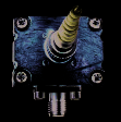
Fig. 3. The experimental setup for the measurement of circuit model elements: (a) The
configuration diagram, (b) The photograph of the packaged SNSPD.
10MHz-6GHz, a Keithley 2400 SourceMeter, and a Janis ST-500 cryostat. Their connection
is illustrated in Fig. 3 (a). The DUT is packaged in an ETP copper housing equipped with
a 40 GHz bandwidth k-connector to maintain the high frequency performance free from the
cryogenic temperature stress. The k-connector dielectric layer is made of air/vacuum rather
than Teflon in SMA connectors that suffers contraction. In addition, the dielectric constant
of Teflon may vary such that it may lead to unwanted variation of the port impedance.
The packaged housing is first plated with nickel followed by gold to improve the thermal
conduction with the cryostat cold plate. The NbN meanderline is electrically connected by
silver epoxy to glue one contact pad to the microwave center pin, and the remaining two pads
to the wall of the housing. The final result of the device package is shown in Fig. 3 (b).
The measurement assumes that any extra time delay arising from interconnections within
the device packaging is negligible, because of two considerations: (1) The S-parameter S 11
can be technically measured at only the reference plane, located at input/output port of the
packaged NbN meanderline. The reference plane is set by calibration with VNA; (2) The
working wavelength (in meters) is much longer than the total electrical wire length (in one
hundredths of a meter) including the packaging and the coplanar waveguide on the substrate.
Thus, the circuit model in conjunction with its mathematical description has been justified.
It is challenging to do S-parameter measurement under cryogenic temperature and high
vacuum because of two limiting factors: (1) We have to limit the amplitude of the ac signal
to avoid the device latching when the dc bias is very close to its critical point; (2) The
interconnection loss along the transmission line, especially the connector loss, weakens the
reflected power. As a result, the ratio of signal to noise becomes extremely low. Since
the standard one-port calibration can be performed only in the range of room temperature
(approximately 25-30 ◦C) and pressure (103 mbar), the forward tracking error terms in a
standard one-port calibration algorithm can not be kept accurate enough, because the portion
of the measuring coaxial cable has been cooled far below its calibrating temperature; and has
been placed in an ambient of high vacuum condition (< 10−5 mbar).
We have observed that the amplitude of Γ in the frequency range experiences about 0.1 dB
variation on average. According to our calculation, Rs should be very sensitive to |Γ| when
the dc bias current is very close to zero, because Rs is expected to be very close to zero.
The associated phase angle variation can be approximated in the complex plane by simple
geometrical relations and the result indicates the phase angle variation is less than 0.6 degree.
Investigating Optoelectronic Properties of the NbN
Superconducting Nanowire Single Photon Detector
269
1.20
1.18
1.18
for QE 2.0% SNSPD
for QE 0.2% SNSPD
1.16
1.16
1.14
k
1.14
1.12
1.12
1.10
ized L
ized Lk 1.10
al 1.08
al 1.08
1.06
orm
orm
N 1.04
N 1.06
1.04
1.02
1.00
1.02
1.00
0.0
0.1
0.2
0.3
0.4
0.5
0.6
0.7
0.8
0.9
1.0
0.0
0.1
0.2
0.3
0.4
0.5
0.6
0.7
0.8
0.9
1.0
DC Current Bias ( β=Ib/Ic)
DC Current Bias ( β=Ib/Ic)
Fig. 4. The measured kinetic inductance for two NbN nanowire meanderlines with different
film quality; solid lines are results from theoretical simulations.
Thus, the inductance measurement can achieve a good accuracy, even though the capacitance
reduces the phase angle as a function of frequency ω.
In the experiment, we treat the bias tee and cryogenic cable as one lossy transmission line.
The calibration is done by setting the reference plane to the end of the cryogenic cable, i.e. the
k-connector input of the packaging. Thus, losses from the cryogenic cable, the bias tee and
interconnecting components, which are in the ambient temperature, have been compensated
by the calibration. The calibration frequency ranges from 10 MHz to 300 MHz. The dc bias
source is programmed in either current or voltage mode. The microwave probing power is set
at -76 dBm, corresponding to 1 μ A peak-to-peak ac current at a 50 Ω coaxial cable. However,
considering the cryogenic cable loss, the effective ac current amplitude at the device side falls
to about 0.25 μ A, which poses much less perturbation to the system during the measurement.
Meanwhile, we have observed that when the frequency is higher than about 70 MHz, the S 11
magnitude variation due to the incident microwave signal becomes negligible. Therefore, the
measurement of circuit elements Lk, C and Rs starts with S 11 frequency points higher than 70
MHz and averages them to the upper frequency limit (in this measurement it is 300 MHz).
Moreover, the choice of calibration power is -30 dBm, whereas the measurement power is set
to -76 dBm. This calibration power level is chosen by considering that the minimum noise
floor for this VNA preamplifier is -110 dBm. If the calibration power is too low, the forward
tracking error term can not be well resolved after the calibration. We can use the data track
smooth algorithm as well when we switch the power level down to -76 dBm. However, the
smoothing data track can not lead to a higher signal to noise ratio. Instead, we can reduce
the IF bandwidth to 10 Hz to increase the measurement accuracy. Based on our experiment,
further decreasing IF bandwidth has no appreciable improvement. In addition, stepped frequency
scanning is adopted in lieu of the default adaptive scan mode. Each stepped frequency has a 1
ms delay to make sure no residue power affects the adjacent frequencies.
3.2 Kinetic inductance measurement results
Initially, we apply the current bias scheme in the measurements.
Fig.
4 shows the
measured kinetic inductance for two identical packaged devices, made of NbN nanowire
meanderlines. Both measurements of Lk have been normalized to their zero bias kinetic
inductance, respectively. The capacitance has been measured in the room temperature via one
port S-parameter measurement. The measured capacitance after postprocessing indicates that
its value is device dependant. In this work, the capacitance for higher quality film nanowire

270
Optoelectronic Devices and Properties
30
IC
1400
(a)
(b)
25
1200
20
1000
)
15
H(n 800
(μA)I 10
L K
600
5
Hot spot plateau
400
0
200
-1
0
1
2
3
4
5
6
7
8
9
10
11
12
-1
0
1
2
3
4
5
6
7
8
9
10
11
12
DC Bias Voltage (mV)
DC Bias Voltage (mV)
Fig. 5. The linkage of the I-V scan and kinetic inductance variation, (a) the I-V curve under
voltage bias scheme; (b) the measured kinetic inductance Lk.
is 1.6 pF; whereas for the lower film quality 1 one, its capacitance is 1.4 pF. On the other hand,
the former has zero bias kinetic inductance at about 210 nH; while the latter is 230 nH. In both
cases, the nonlinear kinetic inductance displays a trend of higher Lk associated with a higher
bias ratio. Detailed discussions on the theoretical background are presented in Appendix A.
The relationship of Lk with respect to the bias current ratio is given by (5); and the simulation
results are plotted as solid curves in Fig. 4.
However, neither in this work nor in the relevant literatures (Miki et al., 2008; Hadfiled et
al., 2007) have shown any abrupt change of Lk when the dc bias current is very close to the
so-called critical current Ic, even when we are able to drive the bias current ratio above 99%.
Since the kinetic inductance Lk by definition should be inversely proportional to the Cooper
pair density of the nanowire condensate, this seems to imply that the Ic may only be a local
effect, possibly a resistive spot somewhere along the nanowire. Further increasing the bias
current above Ic will cause device permanent latching .
Based on the preceding analysis, we switch our dc bias scheme into voltage bias. Now all of
the measurement conditions are kept the same except the bias method. Fig. 5 demonstrates
the linkage between the different I-V regimes and the kinetic inductance Lk of the NbN
meanderline. The curve shows that even when the bias current decreases after Ic, the kinetic
inductance increases constantly with the increasing bias voltage. This suggests that Cooper
pairs are proportionally accelerated by applied voltages without apparent resistance barriers
along the meanderline path, until the hotspot formation plateau occurs. At that transition
point, the kinetic inductance changes very abruptly to 1500 nH at 4.2 K. In order to see the
connection of the increasing kinetic inductance Lk with the series resistance Rs, Fig. 6 shows
the measured Lk and Rs at each bias voltage point. The figure suggests that when the bias
voltage surpasses the point where Ic occur