0.059
?
2.439
0.144
0.056
2.447
0.136
0.053
ZnTe zinc
blende 2.39
2.185
0.21
0.088
Te(g) 90o partials?
2.148
0.24
0.100
CdTe
zinc
blende
1.61 1.48 0.13 0.081 Te(g)
90o partials
GaAs zinc blende
1.52
1.13
<0.2
<0.132
As(g) 90o partials
Table 1. Emission bands related to dislocations
Figure 7 summarizes the atomistic structure of dislocations on a basal plane introduced at
elevated temperatures, proposed in this ZnO work. 90o partial dislocations in the dissociated
60o dislocations would form a defect level of 0.3 eV depth acting as radiative recombination
center, while the screw and edge dislocations form a defect level near the mid gap acting as
non-radiative recombination center, similar to wurtzite GaN (Albrecht et al, 2002).
Fig. 7. A schematic view of the defect levels of misfit dislocations in ZnO
Misfit dislocations in ZnO introduced at elevated temperatures do not influence the
emissions except the dislocation-related emissions, as in Fig. 2a. On the other hand, almost
all emissions in ZnO are suppressed due to the introduction of misfit dislocations at room
temperature (Coleman et al, 2006, Takkouk et al, 2005). Since those dislocations are similar
in type, the atomistic structure of a dislocation would be modified at elevated temperatures,
presumably due to an interaction of the dislocation with point defects. Indeed, a dislocation
involving point defects is the candidate for the 3.1 eV emission band (Ohno et al, 2008b).
Also, the intensity of the green (2.43 eV) and yellow (2.18 eV) emissions, associated with O-
and Zn-vacancies (Zhao et al, 2005), varies when dislocations modify their structure via their
glide (Figs. 5 and 6). This characteristic of ZnO may be an advantage over GaN, since all
emissions in GaN are suppressed when dislocations are introduced even at elevated
temperatures (Yonenaga et al, 2006), as well as at room temperature. (Kucheyev et al, 2000).
The interaction of dislocations with point defects is a key to elucidate the influence of
dislocations on the optoelectronic properties in ZnO. In order to understand the properties
252
Optoelectronic Devices and Properties
at an atomistic level, it is needed to determine an individual dislocation with a higher spatial
resolution, as well as with a high spectral resolution. Near-field optical measurements in a
TEM (Fig. 8) will be a unique technique to reveal the subject.
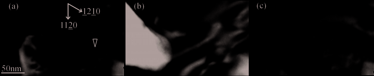
Fig. 8. A preliminary result for in-situ examination of a photo-induced glide of an individual
dislocation in ZnO. TEM images of the screw dislocation indicated with the arrowhead in
(a); before (a), under (b), and after (c) the illumination of a near-field light with photon
energy of 2.41 eV. The broken curve in (c) indicates the dislocation line before the
illumination. (Ohno, 2010a)
It is shown that transmission electron microscopy under light illumination is available to
determine quantitatively the defect levels acting as non-radiative, as well as radiative,
recombination centers, with a high spatial resolution. By means of this technique, combined
with another in-situ techniques such as environmental TEMs (e.g., Yoshida et al, 2008, 2009)
and in-situ electrifying (e.g., Nogami et al, 2009, Kohno et al, 2009), the dynamic properties
of nanostructures and defects under electronic excitation will be determined.
3.2 Quantum nanostructures in middle gap semiconductors
After the successful fabrication of quantum wells based on middle gap III-V compound
semiconductors including AlGaAs, around 1970, various kinds of quantum nanostructures
have been fabricated. For example, by using the differences in the surface migration of
adatoms and using the Stranski-Krastanov growth, quantum wires and quantum dots have
been self-organized. Also, by means of modern crystal-growth techniques such as metal-
organic chemical-vapor deposition and molecular-beam epitaxy, superlattices based on
periodic changes of either material compositions or doping patterns have been grown. Such
quantum nanostructures have potentials for enhancing the device performance, and also
their electron confinement produces quantum electronic states which provide an important
system for fundamental physics.
Recently, superlattices based on periodic changes of crystal directions, i.e., twinning
superlattices (Ikonic et al, 1993), have been proposed in III–V (Xiong & Eklund, 2006, Ohno et
al, 2007b, Algra et al, 2008, Bao et al, 2008), II-VI (Ikonic et al, 1996), and VI (Hibino et al, 1998,
Fissel et al, 2006) semiconductors and in metals (e.g., Kobayashi & Uchihashi, 2010). It is
expected that they can offer as much versatility in tailoring the miniband structure as there
exists in heterostructure-based superlattices (e.g., Ikonic et al, 1993, Nakamura & Natori, 2006).
In this subsection, the optoelectronic properties of twinning nanostructures self-organized in
indirect gap Al0.5Ga0.5As epilayers, revealed by CL spectroscopy in a TEM, are reviewed.
An Al0.5Ga0.5As epilayer without extended defects is traditionally grown on a substrate that
is flat and electrically neutral; the substrate is oxidized intentionally, to form a flat interface
between the oxide and the substrate, and the oxide is then removed by the annealing in an
As atmosphere, for fear of the sublimation of As atoms on the substrate. On the other hand,
when a substrate is not treated the pretreatments, multiple twin boundaries are induced on
In-Situ Analysis of Optoelectronic Properties of Semiconductor Nanostructures
and Defects in Transmission Electron Microscopes
253
the substrate; the boundaries are induced in an epilayer grown on a rough As-deficient
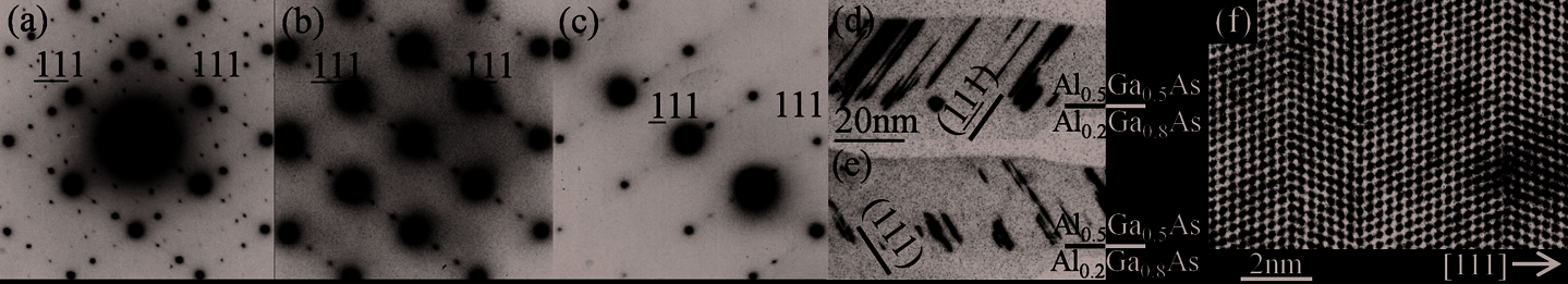
surface (Ohno et al, 2008c). Twin boundaries of Σ3 type are formed on (111) and (111) (Fig.
9). No compositional fluctuation is detected around the boundaries, indicating that
heterostructures, such as AlxGa1-xAs/AlyGa1-yAs superlattices and impurity agglomerates,
are not self-organized around the boundaries.
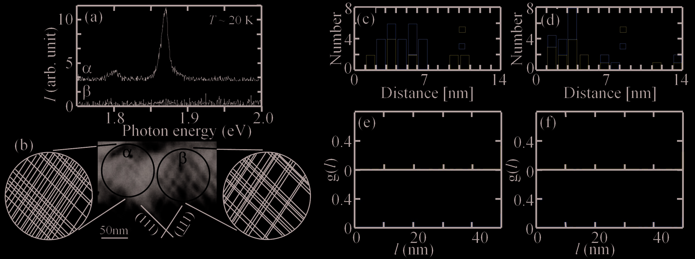
Fig. 9. Diffraction patterns of a twinned Al0.5Ga0.5As epilayer taking along (a) [110], (b) [011],
and (c) nearly [011]. TEM images taking with a twin spot at (d) 1/3, 1/3, 5/3 and (e) 1/3,
1/3, 5/3. (f) A high-resolution TEM image of twin boundaries. (Ohno et al, 2007b)
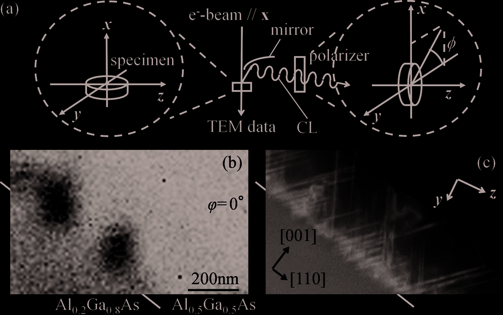
Fig. 10. (a) The experimental setup for polarized CL spectroscopy. (b) A panchromatic CL
intensity map and (c) the corresponding bright-field TEM image of a twinned Al0.5Ga0.5As
epilayer grown on an Al0.2Ga0.8As. (d)-(g) Monochromatic CL intensity maps, and (h)-(i) the
corresponding dark-field TEM images in which the locations of boundaries are indicated
with the solid lines. The photon energy of the CL light is; (d, e) 1.82 eV or (f, g) 1.85 eV. φ =
(d, f) 0o or (e, g) 90o. (h) or (i) is, respectively, taken with a twin spot of α or β in (j). (k)
Polarized CL spectra for φ = 0o and 90o from the square area of Fig. (h). (Ohno et al, 2007b)
254
Optoelectronic Devices and Properties
CL mapping measurements reveal that (Ohno et al, 2007b), a CL light is emitted from a
twinned layer, and the intensity is stronger in comparison with the band-to-band emission
in direct-gap Al0.2Ga0.8As (Figs. 10b-10c), even though the layer is an indirect gap
semiconductor. A CL light is emitted from an area in which many parallel boundaries are
arranged at similar intervals of nanometer length, and no CL light is detected in the other
areas (Figs. 10d-10i).
The distribution of the boundaries in a light source is characterized with the intervals
between the nearest-neighbor boundaries and the distribution function of boundaries g( l)
(Ohno, 2010b). g( l) is defined as the number of boundaries in the range of l to l+Δ l with the origin at a boundary divided by the number of boundaries N, similar to a distribution
function for an extended defect (Ohno et al, 2007a): g( l) = 1/ N Σ Ni=1 n( l)/Δ l in which n( l) is the number of boundaries in the range of l to l+Δ l for the i-th reference boundary, l is the distance from the i-th reference boundary. Figure 11 shows an analysis of a light source,
indicated with α in Fig. 11b. There is no translational symmetry in the arrangement of the
boundaries, even though the intervals are much the same (Fig. 11c). However, they do not
distribute randomly but orderly in a short range. There are three peaks arranged at similar
intervals (peaking at the intervals of 2–5, 7–9 and 12–14 nm) in the distribution function for
the (111) boundaries (Fig. 11e). Therefore, four or more (111) boundaries are arranged with
the period of about 4 nm. Similar results are obtained at the areas from which a
monochromatic CL light is emitted.
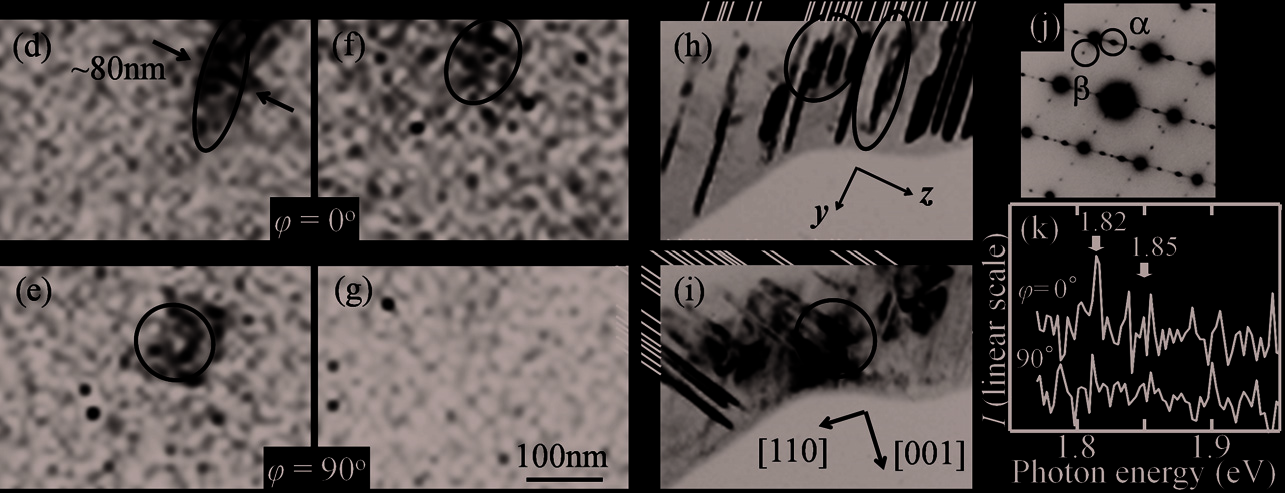
Fig. 11. (a) CL spectra obtained from the encircled areas α and β in (b) [the insets in (b) show
the locations of the boundaries in the areas]. (c) or (d), respectively, shows the histogram of
the intervals between the nearest-neighbor boundaries in α or β. (e) or (f), respectively,
shows the distribution function of boundaries in α or β. (Ohno, 2010b)
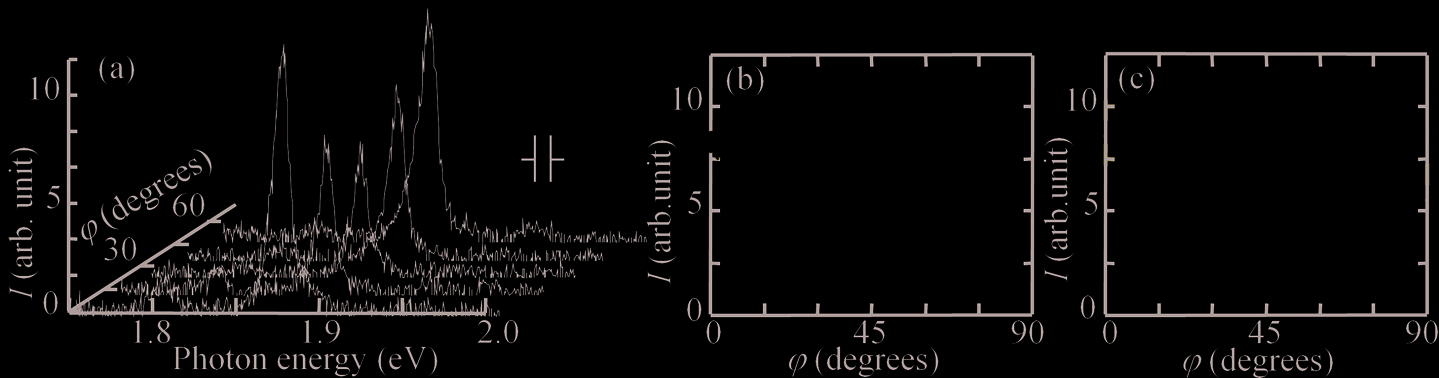
The intensity profile of a CL light emitted from a set of parallel boundaries vs the photon
energy is fitted with a Lorentz function (e,g., Fig. 11a), and the half-width at half-maximum
(5–6 meV) is narrower in comparison with the band-to-band emission in direct-gap
Al0.2Ga0.8As (9–10 meV) and with an impurity emission (about 20 meV). The CL light is
polarized parallel to the boundaries (Figs. 10d-10i, Fig. 12), and the photon energy increases
with decreasing the interval of the boundaries. Those results indicate that a light source is a
set of parallel twin boundaries ordered in a short range.
By means of temperature T-dependent CL spectroscopy (Ohno, 2010b), the energy level
induced by ordered boundaries is determined (Fig. 13). The intensity of a CL light with the
photon energy of E L, I can be fitted with a function: I( T) = I 0/[1 + C exp( ΔE/kT)] where ΔE is
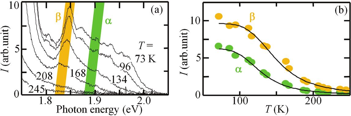
In-Situ Analysis of Optoelectronic Properties of Semiconductor Nanostructures
and Defects in Transmission Electron Microscopes
255
the activation energy for the thermal quenching process and I 0 or C is a constant (Holtz et al,
1985). ΔE for a CL light due to ordered boundaries is higher in comparison with bound
excitons, and it increases with decreasing E L. The estimated energy is close to the difference
between the band gap energy E g and E L, indicating that the light is emitted via an electronic
transition between an energy band and a defect level associated with the boundaries;
thermal escape of the carriers trapped in the level is responsible for the quenching.
Fig. 12. (a) Polarized CL spectra for different φ obtained from α in Fig. 11b. The experimental
setup is similar to that in Fig. 10a, and the specimen is set so that the z axis is parallel to
[001]. The CL intensity I vs φ; the z axis is parallel to (b) [001] or (c) [110] (Ohno et al, 2007b) Fig. 13. (a) CL spectra obtained at various temperatures T. (b) T-dependence of the CL
intensity for the emission line α and that for β in (a). (Ohno, 2010b)
Electron flux-dependent CL spectroscopy reveals that (Ohno et al, 2007c), the photon energy
of a CL light due to a set of ordered boundaries is independent of electron flux. The
intensity obeys a power law (Schmidt et al, 1992), and the power α is about 2.0. These results
indicate that the CL light is emitted via a band-to-band electronic transition, rather than a
donor–acceptor pair recombination (α < 1) and an excitonic transition (1 < α < 2).
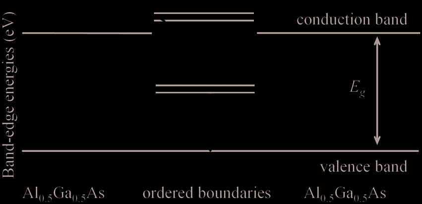
Figure 14 shows the energy diagram based on a twinning superlattice theory (Ikonic et al,
1993). Suppose a twinning superlattice structure, which forms a narrow miniband whose
energy is lower than the energy at the conduction band edge, is embedded in the indirect
gap Al0.5Ga0.5As crystal. According to the model, an intense monochromatic CL light with
photon energy E L, polarized parallel to the boundaries, is emitted via the direct transition
between the miniband and the valence band. The thermal escape of electrons from the
miniband into the conduction band in the adjacent Al0.5Ga0.5As crystal is responsible for the
quenching of the CL emission, and the activation energy for the quenching Δ E is E g− E L.
It is shown that CL spectroscopy in a TEM is available for the quantitative analyses of the
optoelectronic and structural properties of nanostructures with a high spatial resolution
(higher than about 80 nm as in Fig. 10d). The technique will be applied to explore novel
256
Optoelectronic Devices and Properties
nanostructures and defects with useful optoelectronic functions, as well as to assess the
functions at an atomistic level, inside semiconductors.
Fig. 14. A schematic view of band-edge energies for an ordered boundaries embedded in an
Al0.5Ga0.5As layer in which no twin boundary exists
3.3 Silicon and related materials as optoelectronic materials
Si and related materials are still the most important semiconductor for various kinds of
photovoltaic and electronic devices. However, small numbers of the optical assessments
have been performed in TEM since Si is an indirect-gap semiconductor. Even though 60o
and Lomer-Cottrell dislocations are believed to act as radiative recombination center (Higgs
et al, 1992, Sekiguchi & Sumino, 1996), they have not been determined in TEM. Some
preliminary optical measurements for Si nanostructures which emit visible light, such as
porous-Si (Itoh et al, 1996) and Si nanowires (Ozaki et al, 1998, 2005, Kohno et al, 2004), have
been performed in a TEM. With a recent progress in optical measurement systems used in
near-infrared region, optoelectronic properties in Si including nanostructures and extended
defects, which would be modified by the interactions with point defects (e.g., Inoue et al,
2008, 2009, Ohno et al, 2009a, 2010), will be elucidated at an atomistic level.
4. Concluding remarks
In-situ optical measurements in TEM are powerful and unique techniques to examine the
atomistic structures of small regions inside materials, with an extremely high spectral
resolution. This in-situ technique in TEM will be applied permanently to discover and assess
various novel nanomaterials.
5. Acknowledgements
This work was partially supported by the Ministry of Education, Culture, Sports, Science,
and Technology, Japan, Grant-in-Aid for Scientific Research (B) #19310072 (2007–2009) and
for Scientific Research on Priority Areas #21016002 (2009-2010), and the Nano-Materials
Functionality Creation Research Project in IMR, Tohoku University.
6. References
Akiba, K.; Yamamoto, N.; Grillo, V.; Genseki, A. & Watanabe, Y. (2004). Anomalous
temperature and excitation power dependence of cathodoluminescence from InAs
quantum dots. Phys. Rev. B. Vol. 70, No. 16, pp. 165322/1-9.
In-Situ Analysis of Optoelectronic Properties of Semiconductor Nanostructures
and Defects in Transmission Electron Microscopes
257
Albrecht, M.; Strunk, H. P.; Weyher, J. L.; Grzegory, I.; Porowski, S. & Wosinski, T. (2002).
Carrier recombination at single dislocations in GaN measured by cathodo-
luminescence in a transmission electron microscope. J. Appl. Phys. Vol. 92, No. 4,
pp. 2000-2005.
Albrecht, M.; Weyher, J. L.; Lucznic, B.; Grzegory, I. & Porowski, S. (2008). Nonradiative
recombination at threading dislocations in n-type GaN: Studied by cathode-
luminescence and defect selective etching. Appl. Phys. Lett. Vol. 92, No. 23, pp.
231909/1-3.
Algra, R. E.; Verheijen, M. A.; Borgstrom, M. T.; Feiner, L. F.; Immink, G.; van Enckevort, W.
J. P.; Vlieg, E. & Bakkers, E. P. A. M. (2008). Twinning superlattices in indium
phosphide nanowires. Nature. Vol. 436, No. 7220, pp.369-372.
Bagnall, D. M.; Chen, Y. F.; Zhu, Z.; Yao, T.; Shen, M. Y. & Goto, T. (1998). High temperature
excitonic stimulated emission from ZnO epitaxial layers. Appl. Phys. Lett. Vol. 73,
No. 8, pp. 122077/1-3.
Bao, J.; Bell, D. C.; Capasso, F.; Wagner, J. B.; Matensson, T.; Tragardh, J. & Samuelson, L.
(2008). Optical properties of rotationally twinned InP nanowires heterostructures.
Nano Lett. Vol. 8, No. 3, pp. 836-841.
Blumenau, A. T.; Fall, C. J.; Elsner, R.; Jones, R.; Heggie, M. I. & Frauenheim, T. (2003). A
theoretical investigation of dislocations in cubic and hexagonal gallium nitride.
Phys. Stat. Sol. (c). Vol. 0, No. 6, pp. 1684-1709.
Bonard, J. M.; Ganiere,J. D.; Vanzetti, L.; Paggel, J. J.; Sorba, L. & Franciosi, A. (1998).
Combined transmission electron microscopy and cathodoluminescence studies of
degradation in electron-beam-pumped Zn1− x Cd x Se/ZnSe blue-green lasers. J. Appl.
Phys. Vol. 84, No. 8. pp. 1263-1273.
Cheng, Y. M.; Herrick, R. W.; Petroff, P. M.; Hibbsbrenner, M. K. & Morgan, R. A. (1995).
Degradation studies of proton-implanted vertical cavity surface emitting Lasers.
Appl. Phys. Lett. Vol. 67, No. 12. pp. 1648-1650.
Coleman, V. A.; Bradby, J. E.; Jagadish, C. & Phillips, M. R. (2006). Observation of enhanced
defect emission and excitonic quenching from spherically indented ZnO. Appl.
Phys. Lett. Vol. 89, No. 8, pp. 082102/1-3.
Donolato, C. & Venturi, P. (1982). Influence of the generation distribution on the calculated
EBIC contrast of line defects. Phys. Stat. Sol. (a) Vol. 73, No. 2, pp. 377-387.
Everhart, T. E. & Hoff, P. H. (1971). Determination of kilovolt electron energy dissipation vs
penetration distance in solid materials. J. Appl. Phys. Vol. 42, No. 13, pp. 5837-5846.
Fissel, A.; Bugiel, E.; Wang, C. R. & Osten, H. J. (2006). Formation of Si twinning-
superlattice: First step toward Si polytype growth. Mater. Sci. Eng. B. Vol. 134, No.
2-3, pp. 138-141.
Farvacque, J. L.; Vignaud, D.; Depraetere, E.; Sieber, B. & Lefebvre, A. (1989). Electrical and
optical properties of dislocations in GaAs. Inst. Phys. Conf. Ser. Vol. 104, pp. 141-150.
Goldstein, J. I. (1979). Principles of thin film X-ray microanalysis. In.: Introduction to
Analytical Electron Microscopy, Ed. Hren, J. J.; Goldstein, J. I. & Joy, D. C. pp. 83-120,
Plenum Press, ISBN 0-306-40280-7, New YorK.
Graham, R. J.; Shaapur, F.; Kato, Y. & Stoner, B. R. (1994). Imaging of boron dopant in highly
oriented diamond films by cathodoluminescence in a transmission electron
microscope. Appl. Phys. Lett. Vol. 65, No. 3, pp. 292-294.
258
Optoelectronic Devices and Properties
Hayazawa, N.; Tarun, A.; Inouye, Y. & Kawata, S. (2002). Near-field enhanced Raman
spectroscopy using side illumination optics. J. Appl. Phys. Vol. 92, No. 12, pp. 6983-6986.
Henderson, B. & Imbusch, G. F. (1989). Optical Spectroscopy of Inorganic Solids, Clarendon
Press, ISBN 0-19-851372-0, Oxford. pp. 315-386.
Hibino, H.; Sumitomo, K. & Ogino, T. (1998). Twinned epitaxial layers formed on Si(111)
√3x√3-B. J. Vac. Sci. Technol. A. Vol. 16, No. 3, pp. 1934-1937.
Higgs, V.; Lightowlers, E. C. & Tajbakhsh, S. (1992). Cathodoluminescence imaging and
spectroscopy of dislocations in Si and Si1− x Ge x alloys. Appl. Phys. Lett. Vol. 61, No. 9,
pp. 1087-1089.
Hilpert, U.; Schreiber, J.; Worschech, L.; Horing, L.; Ramsteiner, M.; Ossau, W. & Landwehr,
G. (2000). Optical characterization of isolated Se(g)-type misfit dislocations and
their influence on strain relief in thin ZnSe films. J. Phys. Condens. Matter. Vol. 12,
No. 49, pp. 10169-10174.
Holt, D. B. & Napchan, E. (1994). Quantitation of SEM EBIC and CL signals using Monte
Carlo electron-trajectory simulations. Scanning. Vol. 16, No. 2, pp. 78-86.
Holtz, P. O.; Monemar, B. & Lozykowski, H. J. (1985). Optical-properties of Ag-related
centers in bulk ZnSe. Phys. Rev. B. Vol. 32, No. 2, pp. 986–996.
Hutchinson, H. J. & Myhajlenko, S. (1984). The cathodoluminescence study of recombination
behavior at dislocations in indium-phosphide. Philos. Mag. B. Vol. 50, No. 4, pp.
L49-L53.
Ikonic, Z.; Srivastava, G. P. & Inkson, J. C. (1993). Electronic properties of twin boundaries
and twinning superlattices in diamond-type and zinc-blende-type semiconductors.
Phys. Rev. B. Vol. 48, No. 23, pp. 17181-17193.
Ikonic, Z.; Srivastava, G. P. & Inkson, J. C. (1996). Electronic structure of natural self-organized
PbS-Bi2S3 twinning superlattices. Phys. Rev. B. Vol. 55, No. 15, pp. 9286-9289.
Ino, N. & Yamamoto, N. (2008). Low temperature diffusion length of excitons in gallium
nitride measured by cathodoluminescence technique. Appl. Phys. Lett. Vol. 93, No.
23, pp. 232103/1-3.
Inoue, K.; Yano, F.; Nishida, A.; Takamizawa, H.; Tsunomura, T.; Nagai, Y. & Hasegawa, M.
(2009). Dopant distribution in gate electrode of n- and p-type metal-oxide-
semiconductor field effect transistor by laser-assisted atom probe. Appl. Phys. Lett.
Vol. 95, No. 4, pp. 043502/1-3.
Inoue, K.; Yano, F.; Nishida, A.; Tsunomura, T.; Toyama, T.; Nagai, Y. & Hasegawa, M.
(2008). Three dimensional characterization of dopant distribution in polycrystalline
silicon by laser-assisted atom probe. Appl. Phys. Lett. Vol. 93, No. 13, pp. 133507/1-3.
Inouye, Y. & Kawata, S. (1994). Near-field scanning optical microscope with a metallic probe
tip. Opt. Lett. Vol. 19, No. 3, pp. 159-161.
Ishikawa, K.; Yamamoto, N.; Tateno, K. & Watanabe, Y. (2008). Characterization of individual
GaAs /AlGaAs self-standing nanowires by cathodoluminescence technique using
transmission electron microscope. Jpn. J. App. Phys. Vol. 47, No. 8, pp. 6596-6600.
Itoh, M.; Yamamoto, N.; Takemoto, K. & Nittono, O. (1996). Cathodoluminescence imaging
of n-type porus silicon. Jpn. J. Appl. Phys.