P² =² (k ² + k ²) = E ( E -ε )
for CdTe ⎪
2
p
2
3
⎭
P is the Kane matrix element given by the relation:
2P²
1
=
(4)
3 ε
2m*
1
where m* = 0.03 m0 is the electron cyclotron mass in HgTe (Tuchendler et al, 1973). For a
given energy E, a superlattice state exists if the right-hand side of Eq. (1) lies in the range
[-1,1]. That implies -π/d ≤kz≤-π/d in the first Brillion zone.
The heavy hole subbands of the superlattice are given by the same Eq. (1) with :
⎧ =²(k ²+k ²)
1
p
⎪-
= E - Λ for HgTe
⎪
2 m*
k
⎪
HH
1
ξ =
r, and r =1
with ⎨
2
(5)
k
⎪ =²(k +k ²)
2
2
p
⎪-
= E for CdTe
⎪
2 m*
⎩
HH
286
Optoelectronic Devices and Properties
m*HH =0.3 m0 (Tuchendler et al, 1973) is the effective heavy hole mass in the host materials.
The band structure computation consists of solving Eq. (1) which represents the dispersion
relations (i.e. finding the values of energy E which are roots of the Eq. (1) for a given value
of the carrier wave vector). Here, we are interested in studying the states of energy of light
particles and heavy holes in HgTe/CdTe superlattice as function of kz when kp=0 and as
function of kp when kz=0 and when kz=π/d. The solving procedure used for studying E as
function kz in the case where kp=0 consists of going, with a steep δE, through the studied
range of energy E and then finding, for each value of E, the value of kz which satisfies the
dispersion relations. The same procedure is used for studying E as function kp in the case
where kz=0 and kz=π/d. It is noteworthy that, for a given value of E, Eq. (1) may have more
than one root in kp. It appears, from Eq. (3)-(5), that the carrier wave vectors k1, k2, and kp
are either real or imaginary (i.e. complex) and then using complex numbers in the
calculation seems to be more adequate.
4. The SL1: HgTe(d1 = 5,6 nm) / CdTe(d2 = 3 nm)
4.1 Theoretical results and discussions
The energy E as a function of d2, at 4.2 K, in the center Γ of the first Brillouin zone and for
our d1 = 1.87 d2, is shown in Fig. 1. (a) (El Abidi et al, 2010). The case of our sample (d2 = 30
Ǻ) is indicated by the vertical broken line. Here the cross-over of E1 and HH1 subbands
occurs. d2 controls the superlattice band gap Eg=EE1-EHH1. For weak d2 the sample is
semiconductor with a strong coupling between the HgTe wells as in the SL1. At the dot
T(d2 = 150 Ǻ, E= 39 meV) the gap goes to zero with the transition semiconductor- semimetal.
When d2 increases, E1 and h1 states drops in the energy gap [0, Λ] and become interface state
with energy
Λε
2
E =
= 34 meV (6)
I
ε + ε
1
2
for infinite d2 obtained from Eq. (1). Then the superlattice has the tendency to become a layer
group of isolated HgTe wells and thus assumes a semimetallic character. The ratio d1/d2
governs the width of superlattice subbands (i.e. the electron effective mass). A big d1/d2, of
4.09 as in the case of the SL2, moves away the material from the two-dimensional behavior.
In the Fig. 1. (b) we can see that the band gap Eg( Γ) increases, presents a maximum at 40
meV and decreases when the valence band offset Λ between heavy hole band edges of HgTe
and CdTe increase. For each Λ, Eg( Γ) increases with T. Our chosen value of 40 meV is
indicated by a vertical dashed line. This offset agrees well with our experimental results
contrary to 0 meV used by (Bastard, 1982) and 360 meV given by (Johnson et al, 1988). The
later offset give Eg (300 K) =135 meV in the right of Fig. 1 whereas, in intrinsic regime, α ∼T-
3/2 and RH T3/2 indicates a measured gap Eg ≈ 190 meV in agreement with calculated Eg(Γ,300
K) = 178 meV.
Fig. 2 shows that, for each d2, Eg ( Γ) decreases when d1/d2 increases. For each d1/d2, when
d2 increases Eg ( Γ) decreases, go to zero at the transition dot T and became negative for a
semimetal conductivity. In the right of Fig. 2, the cut-off wavelength |λc| diverge at T with
d2=54 Ǻ, 100 Ǻ, 150 Ǻ,… respectively for d1/d2=4.09, 2.67, 1.87, … Thus, the transition goes
to high d2 when d1/d2 decreases. In the case of our samples the transition occurs,
respectively, at d2 =150 Ǻ and 54 Ǻ in the SL1 and the SL2.
Band Structure and Magneto- Transport Properties in II-VI Nanostructures
Semiconductors. Application to Infrared Detector Superlattices
287
2 0 0
H g T e /C d T e
d = 1 .8 7 d
1
2
T = 4 .2 K
E
E
E
1
2
3
(a )
1 0 0
)ev
T
mE(
H H 1
h 1
0
H H 2
h 2
0
1 5 0
3 0 0
d (A )
2
0
40
80
120
160
200
240
280
320
360
400
200
200
180
180
160
T = 300 K
160
140
140
)
eV
120
120
m
T = 77 K
100
100
Γ) ( (
E g
80
80
60
60
HgTe/CdTe
T = 4.2 K
40
40
56 Å / 30 Å
(b)
20
20
0
0
0
40
80 120 160 200 240 280 320 360 400
Λ
(meV)
Fig. 1. (a) Energy position and width of the conduction (Ei), heavy-hole (HHi), and the light-
hole (h1) subbands calculated at 4,2 K in the center Γ of the first Brillouin zone as a function
of layer thickness d2 for HgTe/CdTe superlattice with d1=1.87 d2, where d1 and d2 are the
thicknesses of the HgTe and CdTe layers, respectively. T is the point of the transition
semiconductor- semimetal. (b) the band gap Eg ( Γ), in the center Γ of the first Brillouin zone,
as function of temperature and valence band offset Λ between heavy holes bands edges of
HgTe and CdTe for the investigated HgTe/CdTe superlattice
288
Optoelectronic Devices and Properties
0
25
50 75 100 125 150 175
0
25
50
75 100 125 150 175 200
600
HgTe/CdTe
1200
T = 4.2 K
d=d
500
1
2
Λ = 40 meV
1000
d=1.87 d
1
2
400
d=2.67 d
1
2
800
eV)
d=4.09 d
300
1
2
600
μm)
(m
|(
E g 200
400
|λ c
100
200
0
0
0
25
50 75 100 125 150 175
0
25
50
75 100 125 150 175 200
d (Å)
2
Fig. 2. Eg ( Γ) and |λc| as function of d2 for various d1/d2 at 4.2 K
HgTe / CdTe
11
56 Å / 30 Å
10
150
9 μ m)
)
(
eV
λ
λ c
8
(mE g
7
1000
100
200
300
T (K)
Fig. 3. Temperature dependence of the band gap Eg and the cut-off wavelength λc, at the
center Γ of the first Brillouin zone
Using the value of the gaps ε1 and ε2 at different temperatures between 4.2 K and 300 K
(Weiler, 1981) and taking P temperature independent, this is supported by the fact that from
Eq. (4) P ≈ εi(T)/m*(T) ≈ cte, we get the temperature dependence of the band gap Eg, in the
center Γ of the first Brillouin zone in Fig. 3. Note that Eg increases from 111 meV at 4.2 K to
178 meV at 300K. We calculated the detection cut-off wave length by the relation
1240
λ ( m
μ ) =
(7)
c
E (meV)
g
Band Structure and Magneto- Transport Properties in II-VI Nanostructures
Semiconductors. Application to Infrared Detector Superlattices
289
In the investigated temperature range 7 μm< λ <11 μm situates our sample as a medium
infrared detector.
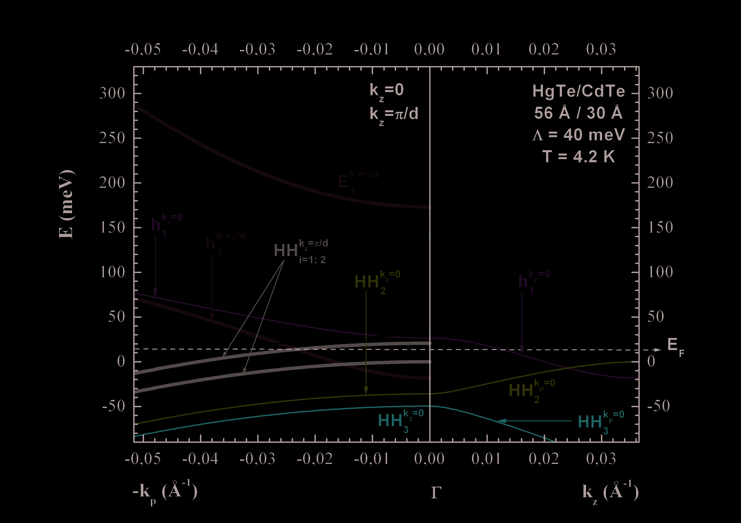
In Fig. 4 we can see the specters of energy E(kz) and E(kp), respectively, in the direction of
growth and in plane of the superlattice at 4.2 K. Along kz the subbands E1 and h1 are wide
and non-parabolic. Along kp, E1 and h1 increase with kp whereas HHn decreases. This yield
Fig. 4. Calculated bands along the wave vector kz in the right and in plane kp(kx,ky) in the
left, of the HgTe/CdTe superlattice at 4.2 K. EF is the energy of Fermi level
to an anti-crossing of HH1 and h1 at kp= 0.01 Å-1 corresponding to a magnetic field of 4
Teslas according to the Formula (13).
4.2 Experimental results and discussions
In Fig. 2, |λc| as function of d2, at 4.2 K, shows that there is a multiple choice of d2 for
medium infrared detectors with |λc|≤ 10µm for each d1/d2. Our choice of d2= 3 nm for
d1=1.87 d2 give a calculated Eg(Γ,300 K) = 178 meV corresponding to Eg (Γ, 300 K) =183 meV
for the well used random alloys Hg0.8Cd0.2Te (Hansen et al, 1982).
In Fig. 5(a) we can see that the angular dependence of the transverse magnetoresistance
vanishes, when the field is parallel to the plane of the SL, indicating a two dimensional (2D)
behavior confirmed by the observation of SDH oscillations in Fig. 7(a).
At low temperatures, the sample exhibits p type conductivity (confirmed by our
thermoelectric power measurements in Fig. 6(b)) with a concentration p=1.84 1012 cm-2 and a
Hall mobility μp = 8200 cm2/Vs in Fig. 5(b) (Nafidi et al, 2004). The decrease of RH (1/T) at
55 K shown by arrow in Fig. 5(c) can be due to coupling between HgTe well (small d1/d2
and d2), to the widening of carrier sub-bands under the influence of the magnetic field
290
Optoelectronic Devices and Properties
HgTe / CdTe
0°
(a )
3 56 Å / 30 Å
30°
T = 4.2 K
50°
2
(a.u)
ΔR
1
70°
90°
00
2
4
6
8
H(T)
104
s)
HgTe / CdTe
/ V
56 Å / 30 Å
2
I =4 μA; B=0.1 T
m
(c
(b)
μ H 103
7.106 )
/ C2m
(c
(c)
R H
106
5.10-3
)
-1 Ω
( σ 0
(d)
10-3 0
100
200
300
103 / T ( K-1 )
Fig. 5. (a) Variation of magnetoresistance of the sample with various angles between the
magnetic field and the normal to the HgTe/CdTe superlattice surface. Temperature
dependence of the Hall mobility (b), weak-field Hall coefficient (c) and conductivity (d)
(Nafidi et al, 2002) in the investigated HgTe/CdTe superlattice
Band Structure and Magneto- Transport Properties in II-VI Nanostructures
Semiconductors. Application to Infrared Detector Superlattices
291
3
HgTe / CdTe
56 Å / 30 Å
T = 4.2 K
p=1.84 1012cm-2
2
0,2
) -1
Δ R (a.u) 1
(T-1 0,1
B m
(a)
0,0
n
0
5
10
15
B (T)
n = 2
h
50
(b)
1
n =1
Λ
n = 0
HH1
HH2
EF
0
n = 0
E (meV)
HgTe / CdTe
56 Å / 30 Å
-50
T = 4.2 K
n =1
n = 2
0
5
10
15
20
B (T)
Fig. 6. (a) Variation of transverse magnetoresistance, with magnetic field of HgTe/CdTe
superlattice, at 4.2 K (b) calculated Landau levels as a function of applied magnetic field of
the HgTe/CdTe SL at 4,2 K. EF is the Fermi level energy
292
Optoelectronic Devices and Properties
and/or to the overlap between involved carriers sub-bands (HH1) and (h1) at (kz, kp) = (0,
0.008 Å-1) and (π/d, 0.023 Å-1) along E(kp) in Fig. 4. Only the later cross over at EF can be
taking into account. This increases the concentration p of holes (decreases of RH (1/T) in Fig.
5 (c)) and decreases of conductivity at 55 K (in Fig. 5 (d)) yielding to a decrease of mobility
(in Fig. 5 (b)) due to the increase of effective mass from mh1 to mHH1. In intrinsic regime (245
K ≤ T ≤ 300 K), the measure of the slope of the curve RH T3/2 indicates a gap Eg=E1-EHH1= 190
meV witch agree well with calculated Eg (Γ, 300 K) =178 meV.
This relatively high mobility μp = 8200 cm2/Vs allowed us to observe the Shubnikov-de
Haas effect (SDH) until 17 Tesla in Fig. 5. (a) (Nafidi et al, 2006). Its well knows that, for a
two dimensional electronic gas, the oscillations of the magnetoresistance is periodic with
respect to 1/B. The period Δ(1/B) is related to the concentration p of the holes by the
relation:
e
p =
(8)
⎛ 1 ⎞
π=Δ⎜ B ⎟
⎝ ⎠
In the insert of Fig. 6(a) we have plot the inverse of the minima’s 1/Bm as a function of the
entire n following the formula:
1
⎛ 1 ⎞⎛
1 ⎞
= Δ⎜ ⎟⎜n + ⎟ (9)
B
⎝ B ⎜
⎠
2 ⎟
m
⎝
⎠
The linear line slope gives Δ(1/B) =0.027 T-1 and p = 1.80 x 1012 cm-2 (in good agreement with
1.84x1012 cm-2 of weak field Hall effect from Fig. 5 (c)).
At low temperature, the superlattice heavy holes dominate the conduction in plane (Fig 4).
The HH1 (and h1) band is parabolic with respect to kp2 (from Fig. 4). That permits us to
estimate effectives masses *
m
=0.297 m , *
m =0.122 m and the Fermi energy (2D) at 4.2
HH1
0
h1
0
K
2
pπ=
E − E
=
= 14 meV (10)
F
HH1
*
mHH1
Around the (222) Bragg reflection in Fig. 7(a), a series of steps are observed corresponding to
the oscillating counterparts described by (Arch et al, 1986). The difference with our results
comes from the monocromacity and the power of their synchrotron source. Our SL1 is a
modulated structure with high quality of interfaces.
The thermoelectric power α measurements shown in Fig. 6(b) (Nafidi et al, 2006) indicate a
p-type conductivity, confirmed by Hall effect measurements in Fig. 5(c). At low
temperature, α ∼T0.8 (in the top insert of Fig. 7(b)) is in agreement with Seebeck effect theory
deduced from the relaxation time resolution of the Boltzmann equation (Seeger, 2002). For
our degenerate holes gas the Seebeck constant is described by the formula:
⎡( k )2 T s 1 ⎤
π
+
B
(
)
⎣
⎦
α =
(11)
3eEF
Band Structure and Magneto- Transport Properties in II-VI Nanostructures
Semiconductors. Application to Infrared Detector Superlattices
293
HgTe/CdTe
56 Å / 30 Å
Reflection (222)
a.u)
(a)
2θ = 21.9°
Counts (
500
550
600
channels
T 0.78
T -1.47
10
(b)
)K
10
μV/
)
α (
10
100
T(K)
μV/K
(α 5
HgTe / CdTe
56 Å / 30 Å
0
0
50
100
150
200
T(K)
Fig. 7. (a) Room temperature X-ray diffraction profile around the (222) Bragg reflection of
the HgTe/CdTe SL. (b) Measured thermoelectric power as a function of temperature of the
HgTe/CdTe superlattice
and the collision time τ ∼ Es-(1/2). This permits us to estimate the Fermi energy at EF = 12 meV
(in Fig. 6(b)) in agreement with the calculated |EF-EHH1|=14 meV with s= 2.06 corresponding
to holes diffusion by ionized impurities. It is relevant here to signal that the maximum of α
at T=55.2 K correspond to the shift of Hall mobility in Fig. 5(b). Here μHH1= 2.434 μh1 at EF.
At T=190 K, a reversal of α sign will occur corresponding exactly to the minimum of the
conductivity σ0 in Fig. 5(d). From p = 1.80x1012 cm-2 of SDH we have deduced the effective
masse of the degenerate heavy holes to be
294
Optoelectronic Devices and Properties
2
∗
πp=
m
=
= 0.308m (12)
HH1
0
EF
(in agreement with the theoretical m*HH1=0.297 m0). We calculated the energy of the Landau
levels (LL) by transposing the quantification rule of the wave vector in the plane of the SL:
2n + 1 eB
2
(
)
k =
(13)
p
=
where n are the quantum orders of LL. The crossing of EF with LL in Fig. 6(b) indicated the
same magnetic field positions as those of the observed SDH oscillations minima Bm in Fig.
6(a).
This HgTe/CdTe superlattice is a stable alternative for application in medium infrared
optoelectronic devices than the random alloys Hg0.8Cd0.2Te because the small composition
x=0.22, with Eg (Γ, 300 K) =183 meV given by the empiric formula for Hg1-xCdxTe (Hansen et
al, 1982).
3