( Γ E 50
50
E (2D)
E (3D)
F
F
40
HH
40
1
h1
30
30
HH2
20
20
HH3
10
10
0
40
80
120
160
200
240
280
T (K)
Fig. 17. Temperature dependence of the energy for the three-dimensional (3D) and two-
dimensional (2D) Fermi levels in the investigated HgTe/CdTe superlattice
E
λ
E
p (cm-2)
µ
g (meV)
c (µm)
F(meV)
p (cm2/Vs)
Theory 4.2 K
Theory 4.2 K
Exper. 4.2 K
Hall ef. 4.2K Hall ef. 4.2K
SL1
111
11 (MIR)
14 (2D)
1.84x10¹² 8200
(p-type)
SL2
3.6
464 (FIR)
32 (3D)
4.51x10¹³ 900
(p-type)
38 (2D)
Table 1. Electronic transport parameters in the investigated two HgTe/CdTe superlattices
302
Optoelectronic Devices and Properties
7. Conclusions
The fundamental main ideas of this work are:
-
HgTe is a zero gap semiconductor (or semimetal) when it is sandwiched between the
wide gap semiconductor CdTe (1.6 eV at 4.2 K) layers yield to a narrow gap
HgTe/CdTe superlattice which is the key of an infrared detector.
-
Before growing our two superlattices, we calculated the bands structures E(d2) and the
gap for each ratio thickness d1/d2. After we choose the SL1 in the semiconductor
conductivity zone and the SL2 at the transition semiconductor-semimetal
We reported here remarkable correlations between calculated bands structures and magneto-
transport properties in two HgTe/CdTe nanostructures superlattices SLi (i=1 and 2). Our
calculations of the specters of energy E(d2), E(kz) and E(kp), respectively, in the direction of
growth and in plane of the superlattice; were performed in the envelope function formalism.
In the SL1, the formalism predicts that the system is semiconductor, for our HgTe to CdTe
thickness ratio d1/d2 = 1.87, when d2 < 14 nm. In our case, d2=3 nm and Eg (Γ, 4.2 K) = 111
meV. In spite of it, the sample exhibits the features typical for the semiconductor type p
conduction mechanism. In the used temperature range, this simple is a medium-infrared
detector, narrow gap and two-dimensional p-type semiconductor.
In the SL2, the formalism predicts that the system is semimetallic, for our HgTe to CdTe
thickness ratio d1/d2 =4.1 for d2 ≥ 3 nm. In our case d2 = 4.4 nm and the gap Eg(Γ,4.2 K) =3
meV corresponding to thermal energy necessary to change the sign of RH(T). In intrinsic
regime, the measurements indicates Eg ≈38 meV in good agreement with calculated Eg (Γ,
300 K) =34 meV = EF (4.2 K)=EI. In spite of it, the sample exhibits the features typical for the
semimetallic conduction mechanism, which agree well with the overlap between carrier
subbands along E(kp) with a quasi-two-dimensional behavior and is a far-infrared detector.
Our HgTe/CdTe superlattices SL1 and SL2 are a stable alternative for application in
infrared optoelectronic devices than the alloys Hg0.8Cd0.2Te and Hg0.66Cd0.34Te respectively.
The theoretical and magnetotransport parameters are in good agreement. Measurements
performed by us on others’ samples indicate an improvement of quality of the material
manifested by higher mobility.
8. Acknowledgements
This work is supported by research budget of University Ibn Zohr in Agadir. We thank Li
Rukang from the School of Chemistry, University of Birmingham, for verifying our X-ray
diffraction Rietveld refinements.
9. References
Arch, D. K.; Faurie, J. P.; Staudenmann, J.L.; Hibbs-Brenner, M. & Chow, P. (1986).
Interdiffusion in HgTe–CdTe superlattices. J. Vac. Sci. Technol. A, Vol, 4, (1986)
(2101-2106), DOI: 10.1116/1.574035.
Bastard, G. (1981). Superlattice band structure in the envelope-function approximation. Phys.
Rev. B, Vol,24, (November15, 1981) (5693–5697), DOI: 10.1103/PhysRevB.24.5693.
Bastard, G. (1982). Theoretical investigations of superlattice band structure in the envelope-
function approximation. Phys. Rev. B, Vol, 25, (June 15, 1982) (7584–7597), DOI:
10.1103/PhysRevB.24.5693.
Band Structure and Magneto- Transport Properties in II-VI Nanostructures
Semiconductors. Application to Infrared Detector Superlattices
303
Cava, R. J. Science 247, pp. 656-662 (1990).
Dingle, R.; Gossard, A. C.; & Wiegmann, W. (1975). Direct Observation of Superlattice
Formation in a Semiconductor Heterostructure. Phys. Rev. Lett., Vol, 34, (May 26,
1975) (1327–1330), DOI:10.1103/PhysRevLett.34.1327.
El Abidi, A.; Nafidi, A.; Chaib, H.; El Kaaouachi, A.; Braigue, M.; Morghi, R.; EL Yakoubi,
E.Y. & M. d’Astuto, (2010). Application of the transition semiconductor semimetal
in modulated nanostructures for communication as infrared optoelectronic device.
Physica B: Physics of Condensed Matter , Vol, 405, (1 February 2010) (936-940),
DOI:10.1016/j.physb.2009.10.019 .
Esaki, L. & Tsu, R. (1970). Superlattice and negative differential conductivity in
Semiconductors. IBM J. Res. Development, Vol., 14, (Jan. 1970) (61-65), ISSN: 0018-8646.
Guldner, Y.; Bastard, G.; Vieren, J.P.; Voos, M.; Faurie, J.P. & Million, A. (1984). Magneto-
optics in a II–VI superlattice: HgTe-CdTe. Surface Science, Vol., 142, (1 July 1984)
(593-597), DOI:10.1016/0039-6028(84)90367-4
Hansen, G. L.; Schmit, J. L. & Casselman, T. N., (1982).Energy gap versus alloy composition
and temperature in Hg1-xCdxTe. J. Appl. Phys, Vol., 53, (10 June 1982) (7099-7101),
DOI:10.1063/1.330018.
Johnson, N. F.; Hui, P. M. & Ehrenreich, H. (1988). Valence-Band-Offset Controversy in
HgTe/CdTe Superlattices: A Possible Resolution. Phys. Rev. Lett. , Vol, 61, (24
October 1988) (1993–1995), DOI: 10.1103/PhysRevLett.61.1993
Kane, E. (1957). Band structure of indium antimonide. Journal of Physics and Chemistry of
Solids, Vol. 1, Issue 4,( January 1957) (249-261). DOI: 10.1016/0022-3697(57)90013-6
Kittel, C. (2001). Introduction to solid stat physics, 3d edition, John Wiley and Sons, Inc, New
York, 333.
Nafidi, Ab.; El Kaaouachi, A.; Sahsah, H.; Nafidi, Ah. (2002). Band structure and magneto-
transport in HgTe/CdTe superlattice. Book of the International Conference on
Theoretical Physics (HT 2002), pp. 274-275, ISBN 3-7643-2433-3, , 22-27 July, Paris,
France Birkhäuser Verlag, Germany.
Nafidi, A.; El Kaaouachi, A.; Nafidi, Ah.; Faurie, J.P.; Million, A.; Piaguet, J. (2002). Some
Transport Properties of HgTe/CdTe Superlattices. Physica status solidi (b), Vol. 229,
(January 2002) (573-576), DOI: 10.1002/1521.
Nafidi, Ab.; EL Abidi, A.; El Kaaouachi, A.; & Nafidi, Ah. (2004). Electronic Band Structure
and New Magneto-transport Properties in p-type Semiconductor Medium-infrared
HgTe / CdTe Superlattice. 27th International Conference on the Physics of
Semiconductors - ICPS-27, AIP Conference Proceedings, Vol. 772, pp. 1001-1002,
DOI:10.1063/1.1994448, July 26-30, 2004, in Flagstaff, Arizona, USA.
Nafidi, A.; El Abidi, A. & El Kaaouachi, A. (2006). Seebeck and Shubnikov-de Haas Effects in
a Two-Dimensional p-type HgTe/CdTe Superlattice. 24th International Conference on
Low Temperature Physics - LT24 , AIP Conference Proceedings Vol. 850,pp. 1359-1360,
ISBN: 0735403473, 10 - 17 Aug 2005, Orlando, FL, USA.
Nafidi A., Bouallal A., El Kaaouachi B., A. and Chaib, H., IEEE Transactions on Applied
Superconductivity. Vol 17 , NO 02, pp 2969-2972, (2007).
Nafidi A., Bouallal B., El Kaaouachi A., Chaib H. and Sahsah H., Advance in Cryogenic
Engineering, Transactions of the International Cryogenic Materials conference-ICMC,
American Institute of Physics, AIP CP986, Vol.54, pp.551-558, (2008).
Nafidi, A., et al, (2011) to be published
304
Optoelectronic Devices and Properties
Sakaki, H.; Chang, L. L.; Sai-Halasz, G. A.; Chang, C. A. & Esaki, L. (1978). Two-dimensional
electronic structure in InAs-GaSb superlattices. Solid State Communications, Vol. 26,
(June 1978) (589-592), DOI:10.1016/0038-1098(78)90770-6
Seeger, K. a (2002). Semiconductor physics: an introduction, Springer, ISBN: 9783540438137,
Edition Number: 8, chap.4, p.121.
Seeger, K. b (2002). Semiconductor physics: an introduction, Springer, ISBN: 9783540438137,
Edition Number: 8, chap.6, p.159.
Tokura, Y. Takagi, H and Uchida, S. Nature 337, pp. 345-347 (1989).
Tuchendler, J.; Grynberg, M.; Couder, Y.; Thomé, H. & Le Toullec R. (1973). Submillimeter
Cyclotron Resonance and Related Phenomena in HgTe. Phys. Rev. B, Vol., 8, (15
October 1973) (3884–3894), DOI: 10.1103/PhysRevB.8.3884.
Weiler, M. H. (1981). Magnetooptical Properties of Hg1-xCdxTe Alloys, In: semiconductors
and Semimetals, Vol., 16, Willardson, R. K. & Beer, A. C. (Ed), (119-191) (Academic,
New York), ISBN: 9780127521169
Part 3
Optoelectronic Measurements in Spatial Domain
15
3D Body & Medical Scanners’ Technologies:
Methodology and Spatial Discriminations
Julio C. Rodríguez-Quiñonez1, Oleg Sergiyenko1, Vera Tyrsa2,
Luís C. Básaca-Preciado1, Moisés Rivas-Lopez1,
Daniel Hernández-Balbuena1 and Mario Peña-Cabrera3
1Autonomous University of Baja California, Mexicali-Ensenada,
2Polytechnic University of Baja California, Mexicali,
3Research Institute of Applied Mathematics and Systems (IIMAS – UNAM)
Mexico
1. Introduction
Medical practitioners have traditionally measured the body’s size and shape by hand to
assess health status and guide treatment. Now, 3D body-surface scanners are transforming
the ability to accurately measure a person’s body size, shape, and skin-surface area
(Treleaven & Wells, 2007) (Boehnen & Flynn, 2005). In recent years, technological advances
have enabled diagnostic studies to expose more detailed information about the body’s
internal constitution. MRI, CT, ultrasound and X-rays have revolutionized the capability to
study physiology and anatomy in vivo and to assist in the diagnosis and monitoring of a
multitude of disease states. External measurements of the body are more than necessary.
Medical professionals commonly use size and shape to production of prostheses, assess
nutritional condition, developmental normality, to analyze the requirements of drug,
radiotherapy, and chemotherapy dosages. With the capability to visualize significant
structures in great detail, 3D image methods are a valuable resource for the analysis and
surgical treatment of many pathologies.
Taxonomy of Healthcare 3D Scanning applications
Application
Epidemiology Diagnosis
Treatment
Monitoring
Anthropometric Growth
Fitness and
Size
Scoliosis
surveys
defects
diet
Abdominal
Shape
Screening
Prosthetics
Obesity
shape
Surface area
Lung volume Drug dosage
Diabetes
Volume
Eczema
Burns
Head Visualization
Melanomas Eating
disorders
Chest Visualization
Facial reconstruction
Hole Body Visualization
Cosmetic surgery
Table 1. Taxonomy of Healthcare 3D Scanning applications
308
Optoelectronic Devices and Properties
1.1 Scanning technologies
Three-dimensional body scanners employ several technologies including 2D video
silhouette images white light phase measurement, laser-based scanning, and radio-wave
linear arrays. Researchers typically developed 3D scanners for measurement (geometry) or
visualization (texture), using photogrammetry, lasers, or millimeter wave (Treleaven &
Wells, 2007).
Taxonomy of 3D Body Scanners
Technique
Measurement
Visualization
Millimeter Wave
Radio Waves
Structured light
Close-range photogrammetry
Photogrammetry
Moire fringe contouring
Digital surface
Phase – measuring profilometry photogrammetry
Laser Scanners
Laser
Laser range Scanners
Table 2. Taxonomy of 3D Body Scanners
In the following section it will be described the diverse measurement techniques (see table 2)
used in medical and body scanners. Listing applications, scanners types and common
application areas, as well of how they operate.
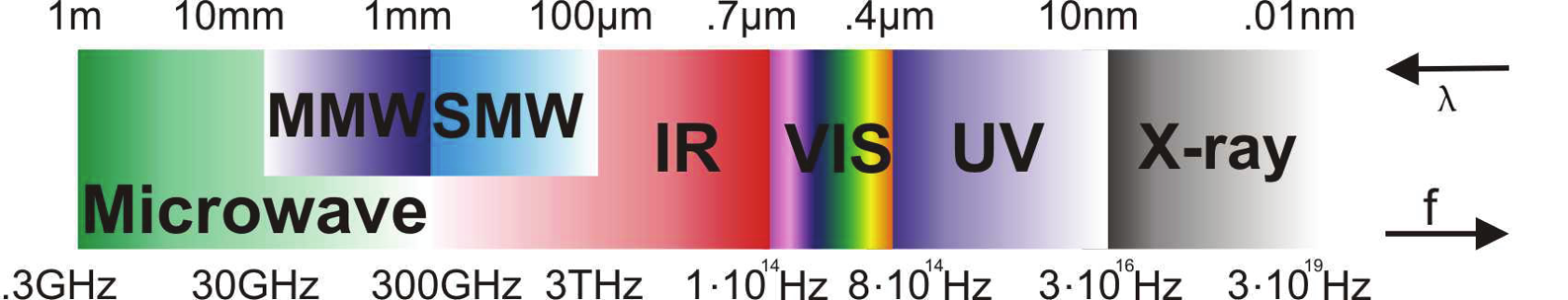
2. Millimeter wave
Millimeter wave based scanners, send a safe, lower radio wave toward a person’s fully
clothed body; most of the systems irradiate the body with extremely low-powered
millimeter waves a class of non-ionizing radiation (see Figure 1) not harmful to humans.
The amount of radiation emitted in the millimeter-wave range is 108 times smaller than the
amount emitted in the infrared range. However, current millimeter-wave receivers have at
least 105 times better noise performance than infrared detectors and the temperature
contrast recovers the remaining 103. This makes millimeter-wave imagine comparable in
performance with current infrared systems.
Fig. 1. Electromagnetic spectrum showing the different spectral bands between the
microwaves and the X-rays
Millimeter (MMW) and Submillimeter (SMW) waves fill the gap between the IR and the
microwaves (see Figure 1). Specifically, millimeter waves lie in the band of 30-300 GHz (10-1
mm) and the SMW regime lies in the range of 0.3-3 THz (1-0.1 mm). MMW and SMW
radiation can penetrate through many commonly used nonpolar dielectric materials such as
3D Body & Medical Scanners’ Technologies: Methodology and Spatial Discriminations
309
paper, plastics, wood, leather, hair and even dry walls with little attenuation (Howald et al.,
2007) (Liu et al., 2007). Clothing is highly transparent to the MMW radiation and partially
transparent to the SMW radiation (Bjarnason et al., 2004). Consequently, natural
applications of MMW and SMW imaging include security screening, nondestructive
inspection, and medical and biometrics imaging. Low visibility navigation is another
application of MMW imaging
Is also true that MMW and SMW open the possibility to locate threats on the body and
analyze their shape, which is far beyond the reach of conventional metal detection portals. A
recently demonstrated proof-of-concept sensor developed by QinetiQ provides video-frame
sequences with near-CIF resolution (320 x 240 pixels) and can image through clothing,
plastics and fabrics. The combination of image data and through-clothes imaging offers
potential for automatic covert detection of weapons concealed on human bodies via image
processing techniques (Haworth et al., 2006). Other potential areas of application are
mentioned below.
Medical: provide measurements of individuals who are not mobile and may be difficult to
measure for prosthetic devices.
Ergonomic: provide measurements and images for manufacturing better office chairs, form-
fitting car and aviation seats, cockpits, and custom sports equipment.
Fitness: provide personal measurements and weight scale for health and fitness monitoring.
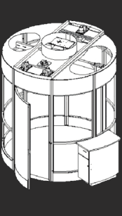
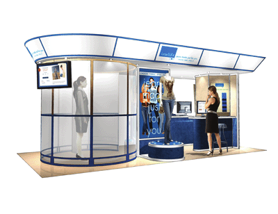
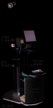
2.1 3D Body millimeter wave scanner: Intellifit system
The vertical wand in the Intellifit system (see Figure 2) contains 196 small antennas that
send and receive low-power radio waves. In the 10 seconds it takes for the wand to rotate
around a clothed person, the radio waves send and receive low-power signals. The signals
don’t “see” the person’s clothing, but reflect off the skin, which is basically water (Treleaven
& Wells, 2007). The technology used with the Intellifit System is safer than using a cell
phone. The millimeter waves are a form of non-ionizing radiation, which are similar to cell
phone signals but less than 1/350th of the power of those signals, and they do not penetrate
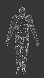
the skin. When the wand's rotation is complete, Intellifit has recorded over 200,000 points in
space, basically x, y, and z coordinates. Intellifit software then electronically measures the
"point-cloud", producing a file of dozens of body measurements; the raw data is then
discarded.
Fig. 2. Intellifit System, cloth industry application and point cloud representation of the
system
310
Optoelectronic Devices and Properties
Although the system is functional to obtain a silhouette of the body, object detection as a
security system and as a tool in the cloth design industry, the problem of this system is the
inaccurate measurements that are closed to 1cm, which makes the system not appropriate
for medical applications.
3. Photogrammetry
Photogrammetry is the process of obtaining quantitative three-dimensional information
about the geometry of an object or surface through the use of photographs (Leifer, 2003).
Photogrammetric theories have on a long history of developments for over a century.
Intensive research has been conducted for the last 20 years for the automation of
information extraction from digital images, based on image analysis methods (Emmanuel,
1999). In order for a successful three-dimensional measurement to be made, targeting points,
each of which is visible in two or more photographs, are required. These targets can be
unique, well-defined features that already exist on the surface of the object, artificial marks
or features attached to the object, or a combination of both types. The accuracy of the
reconstruction is directly linked to the number and location of the targets, as well as number
of photographs and camera positions chosen. Intricate objects generally require more targets
and photographs for a successful reconstruction than do flat or near-flat surfaces. (Leifer,
2003). The latest shift in photogrammetry has been the passage to fully digital technologies.
In particular, low cost digital cameras with high pixel counts (> 6 mega-pixels image
sensors), powerful personal computers and photogrammetric software are driving a lot of
new applications for this technology. (Beraldin, 2004). As shown in Table 2, the
measurement photogrammetry techniques can by refer as show below.
3.1 Structured-light systems
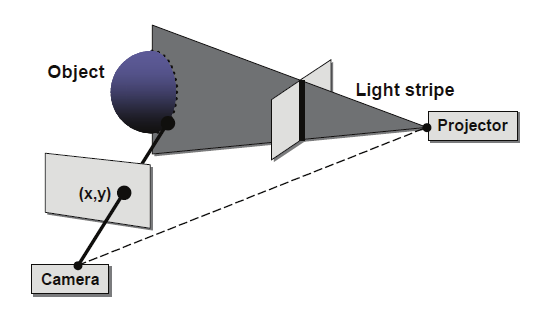
One of the simplest systems consists of a projector that emits a stripe (plane) of light and a
camera placed at an angle with respect to the projector as shown in Figure 3. At each point
Fig. 3. Schematic layout of a single-camera, single-stripe-source triangulation system
in time, the camera obtains 3D positions for points along a 2D contour traced out on the
object by the plane of light. In order to obtain a full range image, it is necessary either to
3D Body & Medical Scanners’ Technologies: Methodology and Spatial Discriminations
311
sweep the stripe along the surface (as is done by many commercial single-stripe laser range
scanners) or to project multiple stripes. Although projecting multiple stripes leads to faster
data acquisition, such a system must have some method of determining which stripe is
which (Rusinkiewicz et al., 2002). There are three major ways of doing this: assuming
surface continuity so that adjacent projected stripes are adjacent in the camera image,
differentiating the stripes based on color, and coding the stripes by varying their
illumination over time. The first approach (assuming continuity) allows depth to be
determined from a single frame but fails if the surface contains discontinuities. Using color
allows more complicated surfaces but fails if the surface is textured. Temporal stripe coding
is robust to moderate surface texture but takes several frames to compute depth and,
depending on the design, may fail if the object moves (Rusinkiewicz et al., 2002).
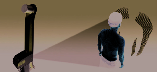
3.1.1 Body and medical 3D structured light scanner: Formetric 3D/4D
The system Formetric 3D/4D is based on structured light projection. The scanning system
consists of four main components: electro-mechanical elevating column for height
adjustment, projector, camera and software. The projection unit emits a white light grid onto
the dorsal surface of the patient standing in a defined way toward the projection device,
which then obtains measuring data on the dorsal profile by means of a video-optic device
from another direction (Hierholzer & Drerup, 1995). Rasterstereography excels by its
precision (methodic error < 0.1 mm) and allows a radiation-free representation of the
profile. For angular data, the reproducibility of an individual rasterstereographic shot is
indicated with 2.8º. The measuring speed of 0.04 seconds can be considered as quick, and
the total dorsal surface is registered simultaneously (Lippold et al., 2007). An automatic
recognition of anatomical structures by means of the connected software provides the basis
for a reconstruction of the three-dimensional profile of the dorsal surface. Figure 4 shows
the Formetric 3D/4D Scann