The numerical method presented is a linear least-square fit
algorithm. The theory of numerical algorithms to extract the emission profile and some
applications are also presented in more detail in Perucco et al. (Perucco et al, 2010). The second
application is the extraction of EGDM parameters from multiple measured current-voltage
curves by a nonlinear least-square algorithm.
4.1 Extraction of emission profiles in OLEDs
The objective of this section is to present and test a numerical fitting algorithm for the
extraction of the emission profile and intrinsic source spectrum. The fitting algorithm is
evaluated by adequate examples and validated on the basis of consistency checks. This
is achieved by an optical model, where a transfer-matrix theory approach for multi-layer
systems is used in combination with a dipole emission model.
The optical model is
implemented in the semiconducting emissive thin film optics simulator (SETFOS) (Fluxim
AG, 2010). With SETFOS, the emission spectrum of an OLED based on an assumed emission
profile and a known source spectrum is generated. The fitting method is then applied to the
calculated emission spectra in order to estimate the emission profile and source spectrum.
The comparison between the obtained and assumed emission profile and source spectrum
is an indication of how successfully the inverse problem can be solved. Sections 4.1.1 deals
with the mathematical derivation of this numerical fitting algorithm. In Section 4.1.2, the
applications or consistency checks are presented.
4.1.1 Theory
The theoretical background of the fitting method is introduced in this section. The method
is linear in terms how the measured emission spectrum is related to the unknown emission
profile. For simplicity the mathematical formulation for the least-square problem is derived
450
Optoelectronic Devices and Properties
for only one emitter. The emitter is characterized by the emission profile. For the moment, it
is also assumed that the emission spectrum is measured in normal direction and therefore
the light is unpolarized. In Section 4.1.1.1, this approach is extended further to multiple
emitters described by several emission profiles and emission spectra measured for several
angles θ. The extracted emission profile Pe( δj) is discretized at N relative positions δj = dj/ L
in the light-emitting layer, where dj is expressed as an absolute position and L is the width
of the layer. The emission spectrum is divided into M wavelengths λi ( i = 1... M). The fitted emission spectrum If ( λi) can be written as
N
If ( λi) = ∑ Ic( λi, δj) · Pe( δj) ,
(27)
j=1
where Ic( λi, δj) is the emission intensity for the wavelength λi and assuming a discrete emission profile (dirac function) at the relative position δj in the layer. The emission intensity
is given by
Ic( λi, δj) = I( λi, δj) · S( λi) ,
(28)
where I( λi, δj) is the emission intensity for emissive dipoles with spectrally constant intensity.
S( λi) is the source spectrum. Between the measured emission spectrum Im( λi) and fitted emission spectrum If ( λi), a residuum can be defined and written as
r 1( λi) = If ( λi) − Im( λi) .
(29)
Equation 29 can be interpreted as a linear least-square problem, written as a system of linear
equations
N
r 1( λi) = ∑ Ic( λi, δj) · Pe( δj) − Im( λi) .
(30)
j=1
The system of equations is normally overdetermined (i.e. M > N) and thus is ill-posed. In
matrix notation, the problem can be formulated as r 1 = A · x 1 − b 1. The matrix A has the
following structure
⎛
⎞
Ic( λ 1, δ 1) Ic( λ 1, δ 2) ... Ic( λ 1, δN)
⎜ I
⎟
A = ⎜ c( λ 2, δ 1) Ic( λ 2, δ 2) ... Ic( λ 2, δN)
⎝
⎟
...
...
...
...
⎠ ,
(31)
Ic( λM, δ 1) Ic( λM, δ 2) ... Ic( λM, δN)
b 1 is a vector containing the measured emission spectrum Im( λi) and the vector x 1
corresponds to the a priori unknown emission profile Pe( δj). The term linear refers to the
linear combination between the matrix A and the vector x 1 of unknown weights. In every
column of the matrix A, an emission spectrum is calculated for a dirac shaped emission profile
at the position δj. The emission profile Pe( δj) at the relative position δj is the weight of the corresponding spectrum, respectively the column. The mathematical task is to minimize the
length of the vector
r 1 .
4.1.1.1 Extracting multiple emission profiles
The most general case of the emission spectrum is determined by the emission profile of
multiple emitters Pe( δk) and emission angles θ
j
l . Given is the emission spectrum measured
at O different angles ( l = 1... O) and the OLED consists of Q different emitters ( k = 1... Q) in Advanced Numerical Simulation of Organic Light-emitting Devices
451
the same or in separate layers. The relation stated in Equation 27, combined with the definition
of the residuum in Equation 30, can be extended to
N
rs, p( λ
) −
2
i, θl ) = ∑ Is, p
c ( λi, δkj, θl ) · Pe( δkj
Is, p
m ( λi, θl ) .
(32)
j=1
Is, p
c ( λi, δk, θ
j
l ) stands for the s-polarized or p-polarized emission intensity at the wavelength
λi. We assume a dirac shaped emission profile at the relative position δk for emitter k and an j
emission angle of θl. Pe( δk) is the emission profile at relative position δ
j
j for emitter k. Equation
32 represents a system of linear equations rs, p =
2
As, p · x 2 − bs, p
2 , where the matrix As, p contains
the s-polarized and p-polarized emission spectra, the vector x 2 contains the information of
several emission profiles and the vector bs, p
2
represents the measured emission spectrum. The
mathematical task is again to minimize the length of the vector
rs, p
2
.
4.1.1.2 Extracting the intrinsic source spectrum
In the case of a single emitter, van Mensfoort et al. (Mensfoort et al., 2010) presented a
method to extract the source spectrum of the light-emitting material. The source spectrum
can be obtained by replacing the emission intensity Is, p
c ( λi, δk, θ
j
l ) by the emission intensity for
emissive dipoles with spectrally constant intensity Is, p( λi, δk, θ
j
l ) in Equation 32. This method
is employed and evaluated in Section 4.1.2.2.
4.1.2 Applications
In this section, the reliability and limitation of the linear fitting method is addressed after it
was mathematically deduced and described in Section 4.1.1. A given intrinsic source spectrum
from a light-emitting material is assumed, together with an emission profile, stating where the
dipoles are located in the device. The effects of quenching are disregarded in the presented
applications below. First, quenching would likely limit the amount of dipoles close to the
electrodes as the lifetime is very short. And secondly, light emitted from the dipoles is also
captured in evanescent modes and therefore, does not couple out into air. Finally, the emission
spectrum is generated by an optical dipole model described by Novotny (Novotny, 1997) and
implemented in the simulator SETFOS (Fluxim AG, 2010). The calculated emission spectrum
is used to solve the least-square problem in Equation 32. This allows the extraction of both,
source spectrum and emission profile. The comparison of the extracted and assumed emission
profile reveals the reliability of the presented algorithm. Throughout this text, an open cavity
is used for the consistency checks. But the method here may also be applied to cavity
and small-molecule based OLEDs. The OLED investigated here has a broad light-emitting
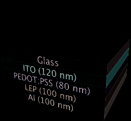
polymer (LEP) of 100 nm. Further, the light-emitting layer is embedded between a 80 nm thick
PEDOT:PSS anode and an aluminum cathode of 100 nm. The device is depicted in Figure 16.
With respect to an experimental setup, the diameter of the semi-sphere glass lens is at least
an order of magnitude larger than the diameter of the OLED. In order to achieve an absolute
quantity of the emission intensity and emission profile, the assumed current density in all
considered consistency checks is 10 mA/ cm 2.
4.1.2.1 Extraction of the emission profile from angularly resolved emission spectra
As an introductory example, this section shows the application to angularly resolved emission
intensity spectra. It compares the extracted emission profile from these spectra to an emission
452
Optoelectronic Devices and Properties
Fig. 16. OLED used to perform the parameter extraction tests with the semi-sphere glass lens.
θ stands for the observation angle.
profile extracted from an emission intensity spectrum measured at normal angle.
The
assumed emission profile is Gaussian shaped, where the peak is set to 0.3 expressed in terms
of a relative position in the emission layer. The width of the Gaussian shape is 20 nm.
3.5
Reference
Fit: Without angle
3
Fit: With angle
]
-1
2.5
s
-3
m
2
27
1.5
1
Profile [10
0.5
0
0
0.2
0.4
0.6
0.8
1
Relative position from anode
Fig. 17. Comparison between the assumed and extracted emission profiles. The emission
profiles were extracted using angularly resolved emission spectra and an emission spectra
measured at normal angle.
The comparison between the extracted and assumed emission profiles in Figure 17 shows an
improvement of the extracted emission profile when angularly resolved emission intensity
spectra are used. The fitted emission intensity spectra match visually perfectly the emission
spectra serving as a measurement, as seen from Figure 18.
4.1.2.2 Source spectrum extraction
This section demonstrates the ability of the least-square algorithm to extract the intrinsic
source spectrum of a light-emitting material. The same assumptions regarding the parameters
of the emission profile are made as in Section 4.1.2.1. The extracted emission profile and source
spectrum can be found on the left, respectively on the right in Figure 19.
It can be seen from Figure 19 that the source spectrum can be extracted very accurately.
The emission profile is also well extracted and even the peak position is reproduced well.
Advanced Numerical Simulation of Organic Light-emitting Devices
453
]
]
-r
50
sr
50 -r sr
80
45 -1
80
45 -1
70
40
nm
70
40
nm
60
35 -2
60
35 -2
50
30
50
30
40
25
40
25
20
20
30
30
Angle [deg]
15
Angle [deg]
15
20
20
10
10
10
5
10
5
0
0
0
0
Fit: Intensity [Wm
Ref: Intensity [Wm
520 540 560 580 600 620 640 660
520 540 560 580 600 620 640 660
Wavelength [nm]
Wavelength [nm]
Fig. 18. Left: Angularly resolved emission intensity spectra serving as a measurement. Right:
Fitted emission intensity spectra by the linear least-square algorithm.
3.5
1
Ref
Fit
3
]
Fit
Ref
0.8
-1 s
2.5
-3
m
2
0.6
27
1.5
0.4
1
Profile [10
Normalized intensity
0.2
0.5
0
0
0
0.2
0.4
0.6
0.8
1
520 540 560 580 600 620 640 660 680 700
Relative position from anode
Wavelength [nm]
Fig. 19. Left: Comparison between the assumed and extracted emission profile. Right:
Relation between the assumed and extracted intrinsic source spectrum by the method
discussed in Section 4.1.1.2.
Illustrated in Figure 20 is the comparison between the assumed and fitted emission spectra,
which are visually also in perfect agreement.
]
]
-r
50
sr
50 -r sr
80
45 -1
80
45 -1
70
40
nm
70
40
nm
60
35 -2
60
35 -2
50
30
50
30
40
25
40
25
20
20
30
30
Angle [deg]
15
Angle [deg]
15
20
20
10
10
10
5
10
5
0
0
0
0
Fit: Intensity [Wm
Ref: Intensity [Wm
520 540 560 580 600 620 640 660
520 540 560 580 600 620 640 660
Wavelength [nm]
Wavelength [nm]
Fig. 20. Left: Angularly resolved emission intensity spectra serving as a measurement to
extract the intrinsic source spectrum from. Right: Fitted emission intensity spectra by the
linear least-square algorithm.
454
Optoelectronic Devices and Properties
4.1.2.3 Extracting multiple emission profiles
Equation 32 explains how multiple emission profiles can be extracted from a measured
emission intensity spectrum. This section illustrates the application of the method to a
multi-emitter OLED. In this example, two emission profiles are extracted. The first assumed
emission profile is Gaussian shaped with a peak at 0.7 and a width of 40 nm. The second
assumed emission profile is also gaussian shaped, where the peak is at 0.3 and the width is
20 nm. Figure 21 shows the extracted and assumed emission profiles, as well as the reference
and fitted emission intensity spectra.
3.5
Ref: 1
60
Ref
3
]
]
Ref: 2
-r
Fit
-1
Fit: 1
sr
s
50
2.5
Fit: 2
-1
-3
m
nm
40
2
-2
27
1.5
30
1
20
Profile [10
0.5
10
Intensity [Wm
0
0
0
0.2
0.4
0.6
0.8
1
400 450 500 550 600 650 700 750
Relative position from anode
Wavelength [nm]
Fig. 21. Left: Showing the differences between the emission profiles from a multi-emitter
OLED. The dotted curves represent the assumed emission profiles, whereas the lines stand
for the extracted emission profiles. Right: Comparison between the measured and fitted
emission intensity spectra.
Despite the fact that the assumed and fitted emission spectra match very well, some
differences in the emission profiles are visible. Nonetheless, the general trend is explained
by the extraction. For the second emission profile, both peak and width can be reproduced
more or less. For the first emission profile, the flat emission profile can be explained as well.
4.2 Extraction of transport parameters from current-voltage curves
The following section deals with the application of a nonlinear least-square fitting algorithm
to extract EGDM parameters from measured current-voltage curves. The nonlinear fitting
algorithm, as well as the EDGM model is implemented in SETFOS. SETFOS is used to generate
three hypothetical measured current-voltage curves at temperatures 320 K, 300 K and 280 K.
All three current-voltage curves are simultaneously fitted for extracting the parameters. The
device considered is a single-layer, hole-only device where the electrical layer has a thickness
of 121.5 nm and the build-in voltage is 1.9 V. The energy diagram of the simulation device is
depicted schematically in Figure 22. The following parameters are of interest: the mobility μp,
the width of the Gaussian DOS σp, the density of chargeable sites N 0 and the workfunction at
the cathode Φ c. Meanwhile, the workfunction at the anode is held constant. The parameters
represent real EGDM parameters as discussed in van Mensfoort et al. (Mensfoort et al., 2008b).
The following parameters are assumed: μp = 1 · 10 − 7 m 2/ Vs, σp = 0.13 eV, N 0 = 6 · 1026 1/ m 3
and Φ c = 3.2 eV. The mobility μp is related to Equation 11 in the following way: μ 0( T) =
μp exp ( − 0.39( σ/( kT))2). The left hand side of Figure 23 shows that the nonlinear least-square algorithm is capable of extracting all four EGDM parameters as the current-voltage curves at
the same temperature match each other visually perfectly.
Advanced Numerical Simulation of Organic Light-emitting Devices
455
Energy Level Diagram
-2
-2.1
-3
PF-TAA
-4
-5
Cathode
-5.2
Energy (eV) -6 Anode
-25
0
25
50
75
100
125
150
Position (nm)
Anode
PF-TAA
Cathode
Fig. 22. Energy diagram for the simulated device. The workfunction at the anode side is held
constant at 5.1 eV, while the workfunction at the cathode side Φ c is being optimized. The
HOMO and LUMO levels are 5.2 eV, respectively 2.1 eV.
1
1
10-2
]
-2
10-2
10-4
10-6
10-4
Ref: T = 320 K