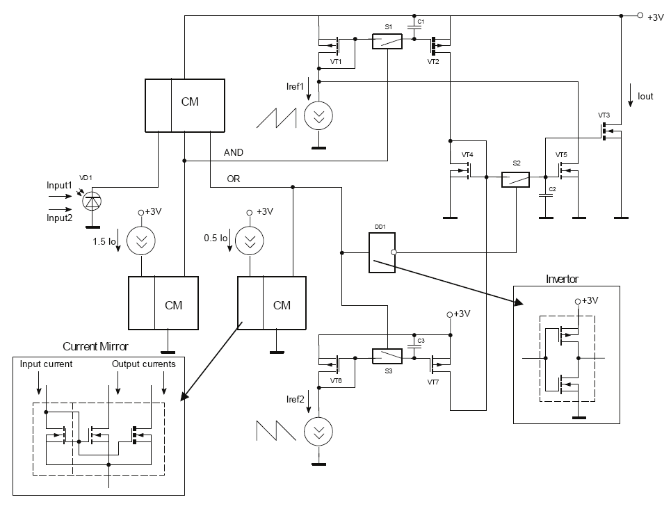
many cases for max-min image processing. The circuit of an inverter on the bases of current
mirrors comparator and its simulation results by PSpice OrCad are shown in Fig.25. The
inverter has current (optical) input and current (optical if a proper LED driver will be
connected) output. AMIS 1.5μm CMOS transistors MOSIS models were used. The supply
voltage is 3V. The circuit shown in Fig.26 can realize both AND and OR functions
depending on the reference current value. Both cases simulation results are shown in Fig. 26.
Input optical signals and corresponding input currents are discrete and equal to 10μA in the
considered case. The number of inputs can be up to 50 and more that is the advantage of the
circuit. If the reference current is less than one input discrete than the circuit execute OR
function. If the reference current is more than the sum of n-1 input discretes than the circuit
executes AND function. If an additional current mirror is connected at the circuit output
then we receive the current output. These circuits are based on current mirrors comparator
and so their performance depends on the comparators and current mirrors performance.
The comparator was considered in our work (Krasilenko et.al, 2004, b) and has the
following characteristics: realized on 1.5μm CMOS transistors; the input currents range –
100nA...100μA; the supply voltage – 3...15V; the relative error is less than 0.5%; the output
voltage time delays is 10…100ns. The using of more advanced CMOS technologies (0.35μm,
0.13μm and so on) can significantly improve the performance, in particular the operation
speed. Time-pulse converters on CMOS current mirrors comparators and on λ-diodes were
considered in our previous works (Krasilenko et.al, 2004, b; Krasilenko et.al., 2003). AND,
OR and OR-NOT function circuits with current output and its simulation results are shown
in fig. 27, 28, 29.
The conception of construction of the family of the offered optoelectronic photocurrent
logical elements (OPLE) consists in the use of a few current mirrors realized on 1.5μm
technology CMOS transistors. Connection of such mirrors with photodetectors and
reference current generators allows also to create circuits realizing the limited difference
operations of continuous current logic and current comparators with potential or current
outputs. Presence of four – ten transistors, one – two photodetectors makes the offered
circuits quite compact and allows their integration in 1D and 2D arrays. The factor of
ramification at outputs and the factor of unification at inputs of the offered elements are
greatly increased. Further we will consider simulation results of the circuits realizing
different Boolean operations including AND, OR, OR-NOT, and others. Thus we will
consider two variants of the circuits: 1- circuits with potential outputs; 2-circuits with logical
current inputs and current outputs.The simulation results on the 1.5μm technology CMOS
transistors showed that the level of logical unit can change from 1 uA to 10 uA for low-
power consumption variants and from 10uA to 100uA for high-speed variants. Signals
delays, values of fronts and cutoffs at operation with impulse logical signals with 1uA
logical unit are not exceed 70-140ns and at operation with impulse logical signals with
100uA logical unit are no more than 4-6ns and the consumption power is 200-400uW.
Design and Simulation of Time-Pulse Coded Optoelectronic Neural Elements and Devices
487
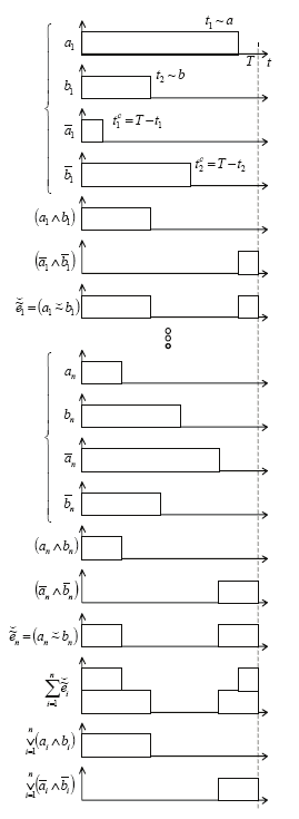
Fig. 23. The time diagram of the scalar-relation vector processor operation
488
Optoelectronic Devices and Properties
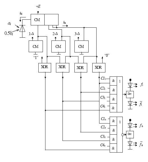
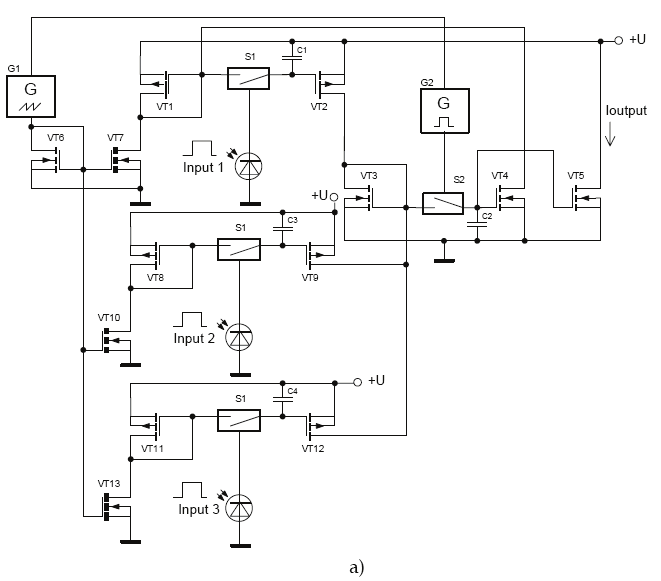
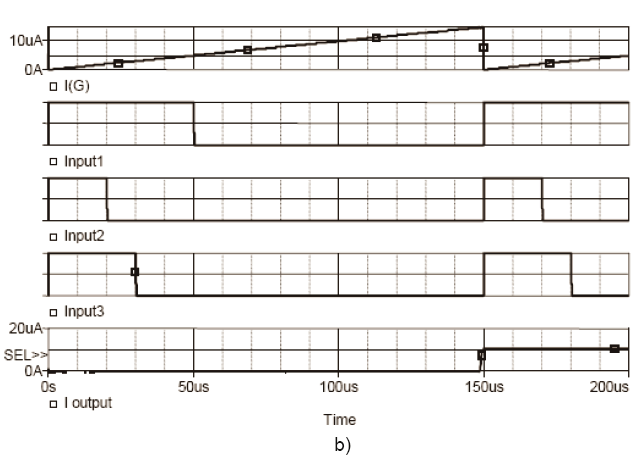
Fig. 24. The universal logical element of two-valued logic
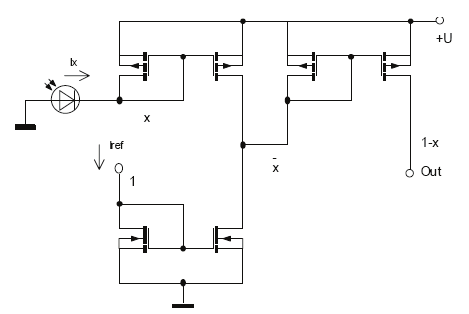
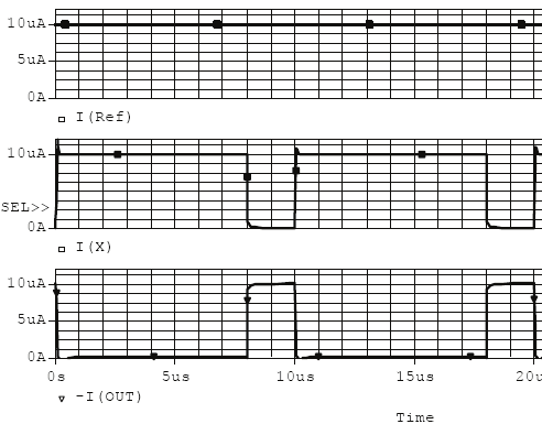
Fig. 25. Inverter circuit on current mirrors and its simulation results
Design and Simulation of Time-Pulse Coded Optoelectronic Neural Elements and Devices
489
20uA
0A
I(IRef)
10uA
0A
I(I1)
10uA
0A
n inputs
I(I2)
+U
I1
I2
10uA
I3
0A
I(I3)
40uA
Iref
Out
0A
I(Input)
SEL>>
0V
0s
5us
10us
15us
V(OUT)
Time
Time diagram of realization of AND function
20uA
0A
I(IRef)
10uA
0A
I(I1)
10uA
0A
I(I2)
10uA
0A
I(I3)
40uA
0A
I(Input)
SEL>>
0V
0s
5us
10us
15us
20us
V(OUT)
Ti
me
Time diagram of realization of OR function
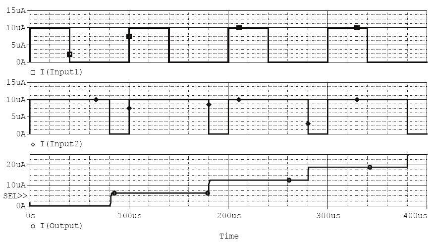
Fig. 26. AND (OR) circuit with potential output on current mirrors and its simulation results
490
Optoelectronic Devices and Properties
2 0 u A
1 0 u A
0 A
I ( R E F 1 )
n inputs
1 0 u A
+U
5 u A
I1
I2
0 A
I3
I ( I 1 )
1 0 u A
5 u A
Cur ent Output
0 A
Iref
I ( I 2 )
1 0 u A
5 u A
0 A
I ( I 3 )
1 0 u A
S E L > >
0 A
0 s
5 u s
1 0 u s
1 5
- I ( O U T 1 )
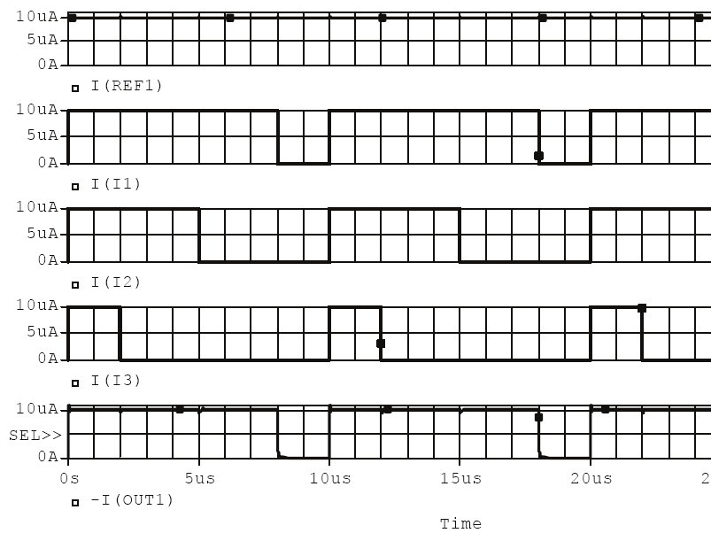
Fig. 27. AND function circuit with current output and its simulation results
n inputs
+U
I1
I2
I3
Cur ent Output
Iref
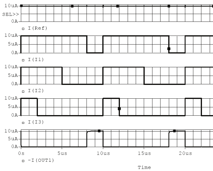
Fig. 28. OR function circuit with current output and its simulation results
+U
Iref
Cur ent Output
n inputs
I1
I2
I3
Fig. 29. OR-NOT function circuit with current output and its simulation results
Design and Simulation of Time-Pulse Coded Optoelectronic Neural Elements and Devices
491
3.6 Spatial-time integrators and equivalence neural elements on their basis
3.6.1 Spatial-time integrators
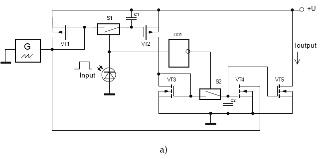
Realization of integrators on current mirrors on CMOS-transistors is perspective due to their
circuit simplicity and compatibility with the well developed CMOS technology of modern
integral digital microcircuits. An integrator of the time type consists of two current mirrors
(Fig. 30). Transistors VT1 and VT2 are intended for integration (algebraic accumulation) of
input signal; VT3, VT4 - for result of integration memorizing. An input optical signal is
transformed in photocurrent with photodiode, and the signal controls keys S1 and S2.Then
the input signal is on, the key is on. If the signal is off, the key if off. Integration is carried
out due to charge of capacities C1 and C2, which hold a value of output current to the end of
transformation cycle. Thus the output current value is determined by the sum of input
signal pulse durations during the period of integration (Fig. 30,b). For example in Fig. 30
value of input signal pulse duration at the first period of integration is 50µs, at the second
period - 100µs, and at the third - 150µs. The output current is proportional to the overall
input signal pulse durations, so after the third period the output current value is
5+10+15=30µA. Thus the circuit carried out integration of input signals during three
periods. The integration circuit has relative error 1…2 %. Input signals photocurrent range
1-100µA, power consumption 100…500 µW, signal period 0.1…1ms, output current delays –
less 1µs Maximal amount of periods, during which the circuit can carry out integration of
input signals, is limited to the maximal possible output current. If value of maximal output
current is 100µA the maximal amount of periods of integration for this circuit is 10 for 10µA
maximal current input signals.
Fig. 30. Integrator circuit (а), time diagrams (b)
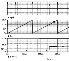
In the same way it is simple to provide the spatial integration of optical signals (Fig. 31).
Input optical signals are converted in photocurrents with photodiodes and the signals
control corresponding keys S1 of selection and storage devices on current mirrors.
Accumulative signal of integration is written in the output device at the end of period by the
control signal of generator G2. Thus the output current is determined by duration of input
signals from every optical channel. For example in Fig. 31 there are three optical channels
and input optical signals are 50µs, 20µs, 30µs accordingly. The output current after the first
period is determined by the pulse duration sum of input signals and it is equal to
5+2+3=10µA. Maximal amount of input signals is determined by the maximal possible
output current. The considered circuits can also perform time integration during some
periods, so it performs spatial-time integration. Circuit simplicity and small power
492
Optoelectronic Devices and Properties
consumption allows to create arrays of such integrators with size 10x10 and more. The range
of input photocurrent is 0.1-10µA, transformation time (period) 100-1000µs, supply voltage
1.5V, average consumption power 150µW per channel.
3.6.2 Neural elements circuits for equivalence and non- equivalence functions
The family of new functions “equivalence” and “non-equivalence” of neuro-fuzzy logic,
which we have elaborated on the based of such generalized operations of fuzzy-logic as
fuzzy negation, t-norm and s-norm are shown in paper (Krasilenko et al., 2002, a). The
functions are prospective for neural networks creation with selforganization and artificial
intelligence properties. New generalized operation of equivalence (non-equivalence)
operation can be written in the following form: t, sE′( a, b) = ( atb) s( a tb = atb s atb , and t-
n
n )
( ) ( )
norm and s-norm of any of their variants can be used. The analysis of the whole spectrum of
all possible t, sE′( a, b) shows, that the following operations are the most interesting in case of certain t- and s-norms (Krasilenko et al., 2002, a). New generalized operation of equivalence
of II type (non-equivalence) can be written in the following form:
s, t E′ ( a, b) = ( asb) t( asb ) , or taking into consideration the law of De Morgan so: s, t E′ ( a b) = (( asb) s asb
= atb s atb
=
E′ a b
= E′ a b
n (
) n) ( ) ( )) ( t, s ( )) t,
,
,
s
( , )
n
n
n
Fig. 31. Spatial-time integrator (а), time diagrams (b)
The II type of operations can be called the operation “non-equivalence” of the I type and
designate it as:
Design and Simulation of Time-Pulse Coded Optoelectronic Neural Elements and Devices
493
t , s NE′( a b) s, t
= E′ ( a b) = ( t,
,
,
sE′( a, b)) .
n
Fig. 32. Equivalence (non-equivalence) function circuit
Fig. 33. Time diagrams of the equivalence circuit operation
494
Optoelectronic Devices and Properties
Thus, the functions determine new generalized operations of comparison (determination of
equivalence or non-equivalence).
The equivalence (non-equivalence) functions can be realized on current mirrors and the
proposed integrators. Output current value Iout is the equivalence of two input optical
signals pulse durations (Fig. 32). In the circuit CMOS current mirrors (CM) with one and
two outputs are used. For example in Fig. 33 input signals pulse durations 40µs and 80µs
(the equivalence of the input signals is 60µs), period 100µs, Io=10µA, output current after the
first period Iout=6uA, after the third period Iout=18µA (Fig. 33), relative error about 3%, as
more than one integrators and current mirrors are used and their errors are summed.
To obtain non-equivalence function circuit the reference saw-tooth current generators Iref1
and Iref 2 must be interchanged. For above mentioned input signals the non-equivalence of
input signals is 40µs (it is the time then signals are different), so the output current after the
first period Iout=4µA, after the third period Iout=12µA.
3.6.3 Weighted and non-linear integration for neural elements circuits for equivalence
and non- equivalence functions
The algebraic spatio-temporal weighted integration of optical signals can be realized by the
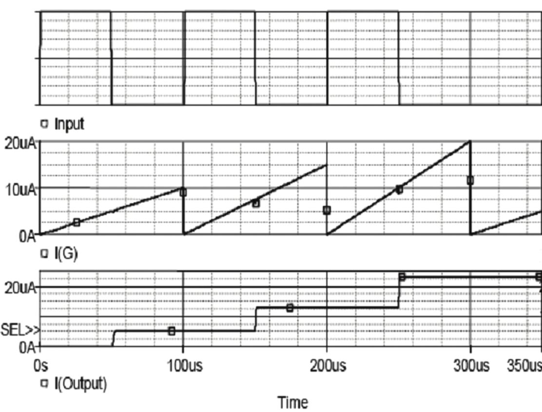
integrator with variable slope angle of saw-tooth current generator G (Fig. 34). For example
in Fig. 35, input signal pulse duration 50µs, period 100µs. The saw-tooth current generator
G determines integration weight. If maximal saw-tooth current is 10uA than transformation
weight is 0.1 µA/µs. So after the first period output current is 5µA. At the second period
maximal saw-tooth current is 10µA that corresponds to transformation weight of 0.15
µA/µs. So the transformation weight is in 1.5 times increased. After the second period the
output current is 5+7.5=12.5µA. At the third period maximal saw-tooth current is 20µA that
corresponds to transformation weight of 0.2 µA/µs. So after the third period the output
current is 5+7.5+10=22.5µA. The considered circuit performs only time weighted integration
of one input signals. But the circuit in Fig. 31 can perform spatio-temporal weighted
integration of multichannel optical input signals if variable angle of slope of saw-tooth
current generator G1 is used. The circuits can be used for neural networks adaptations.
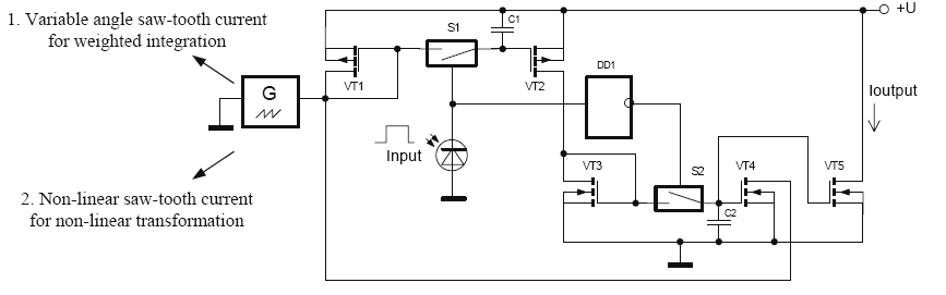
Fig. 34. Weighted or non-linear integrator
Non–linear signal transformation can be realized with the integrator circuit Fig. 34 if a non-
linear saw-tooth current generator is used. For example in Fig. 36 input signal pulse
durations are 20µs, 50µs, 80µs, and period 100µs. An exponential function for saw-tooth
current generator G is used (Fig.36). So we get exponential transformation of input signals.
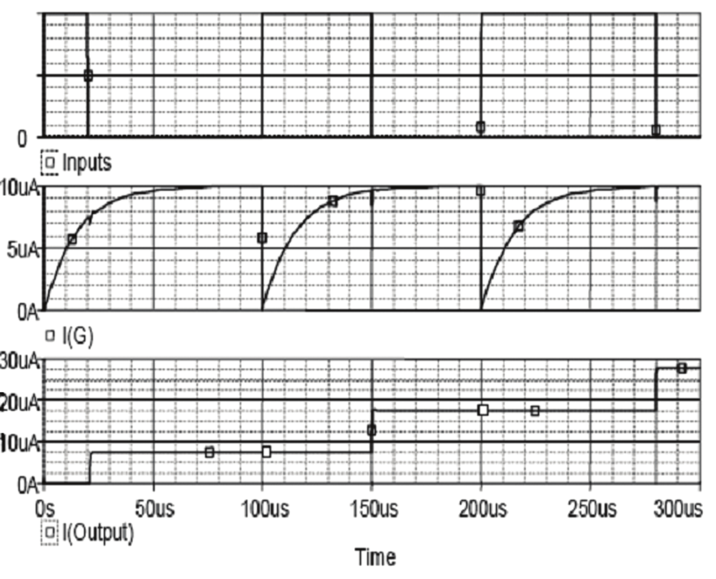
Design and Simulation of Time-Pulse Coded Optoelectronic Neural Elements and Devices
495
After the first period the output current is 7.5µA, after the second period the output current
is 7.5+9.5=17µA, and after the third period the output current is 7.5+9.5+10=27µA. Thus in
spite of identical input signals there are different corresponding output current values. The
circuit can be used for non-linear neural networks activation functions. The non-linear
transformation signals function is determined by a non-linear function of saw-tooth current
generator G.
Fig. 35. Time diagrams of weighted integration
Fig. 36. Time diagrams of non-linear signal transformation
496
Optoelectronic Devices and Properties
4. Conslusion
We consider design and hardware realizations of optoelectronic logical elements of two-
valued logic with current inputs and current outputs on the basis of CMOS current mirrors.
In the chapter we consider the whole family of the offered circuits, show the simulation
results and possible prospects of application of the circuits in particular for time-pulse
coding for multivalued, continuous, neuro-fuzzy and matrix logics. We consider neurons
design and simulation results of multichannel spatio-time algebraic accumulation -
integration of optical signals. Advantages for nonlinear transformation and integration are
shown. The integrator-neuron is based on CMOS current mirrors and comparators. The
performance: consumable power – 10…500 μW, signal period– 0.1…5µs, input optical
signals power – 0.2… 20 μW; time delays – less 0.01-1μs, the number of input optical signals
- 2…64 and more, integration time – 10…100 of signal periods, accuracy or integration error
– about 1%-10%. A biologically motivated concept and time pulse encoding principles of
continuous logic photocurrent mirrors and sample-storage devices with pulse-width
photoconverters have allowed us to design generalized structures for realization of a family
of normalized linear vector operations “equivalence”-“nonequivalence”.
5. References
Ahadian J.F., Fonstad C.G., Epitaxy on electronics technology for monolithic optoelectronic
integration: foundations, development and status, Opt. Eng., 37(12), pp. 3161-3174,
1998.
Antamonov Y.G., Principles of neurodynamics, Naukova dumka, Kiev, 1974.
Awwal A.A., Iftekharuddin K.M., Computer arithmetic for optical computing, (Special
Section), Opt. Eng., Vol. 38(3), pp. 400-513, 1999.
Bardachenko In. F., Kolesnickiy of O. K., Vasileckiy S., Timer neuron elements and
structures. UNIVERSUM-Winnitsa, 2004. – 126p.
Baukens V., Thienpont H., Goulet A. , et al, 2D parallel optical data input for arrays of
optoelectronic transceiver elements. Optical processing and computing , pp15-16,
October 1997.
Berger Christoph, Collings Neil, Gehriger Daniel, Recurrent Optical Neural Network for the
Study of Pattern Dynamics, Proc. SPIE, Vol. 3402, pp.233-244, 1997.
Freeman James and Skapura D.M., Neural Networks: Algorithms applications and
programming techniques, Addison-Wesley Publishing Company, 1992.
Guilfoyle P.S., McCallum D.S., High-speed low-energy digital optical processors, Opt. Eng.,
35(2), pp. 436-442, 1996.
Huang Kung-Shiuh, Keith Tenkins B., Sawchuk Alexander A.. Image algebra representation
of parallel optical binary arithmetic , Aplied Optics.– 1989.– Vol. 28, N6. – P.1263-
1278.
Huang H., Itoh M., Yatagai T., Optical scalable parallel modified signed-digit algorithms for
large-scale array addition and multiplication using digit-decomposition-plane
representation, Opt. Eng., Vol. 38(3), pp. 432-440, 1999.
Klir G.I. and Folger T.A., Fuzzy sets, Uncertainty and Information, Prentice-Hall,
Englowood Cliffs, NI, 1998.
a, Krasilenko V.G. etc., Structure of optoelectronic processors of parallel type for image
processing, New electronic installations and devices, Moscow, 1988.
Design and Simulation of Time-Pulse Coded Optoelectronic Neural Elements and Devices
497
b, Krasilenko V.G., Optoelectronic structures in information-measuring systems for image
processing: Dissertation for the degree of cand. of tech. science. – Vinnitsa, 1988.
a, Krasilenko V.G. et al., Author certificate of USSR N1668984, Arrangement for logical
image processing , Bulletin of inventions, N26, 1991.
b, Krasilenko V.G., Kolesnitsky O.K., Dubchak V.N., Creation principles and circuitry
construction question of multichannel arrangements and systems for parallel image
analysis and processing, Proc. 1-st All-Union Meeting on Pattern recognition and image
analysis, Minsk, Part 3, pp. 83-87, 1991.
Krasilenko V.G., Dubthak V.N., Author certificate of USSR N1711140, Optoelectronic
arithmetic device, Bulletin of inventions, N5, 1992.
a, Krasilenko V.G. et al, Creation opportunities of optoelectronic continuous logic neural
elements, which are universal circuitry macrobasis of optical neural networks,
SPIE, Vol. 2647, pp. 208 – 217, 1995.
c, Krasilenko V.G. et al., Lines of optoelectronic neural elements with optical
inputs/outputs based on BISPIN-devices for optical neural networks, Proc. SPIE,
Vol. 2647, pp. 264 – 272, 1995.
e, Krasilenko V.G., Boguhvalsky A.K., Volosovich A.E., The simulation of information
processing algorithms in optical neural networks in training and recognition
models, Proc. SPIE, Vol.2647, pp.307 – 312, 1995.
Krasilenko V. G., Bogakhvalskiy A.K., Magas A.T.. Equivalental Models of Neural Networks
and Their Effective Optoelectronic Implementations Based on Matrix Multivalued
Elements. Proc. SPIE, Vol. 3055, pp. 127-136, 1996.
a, Krasilenko V.G. et al., Continuos logic equivalental models of Hamming neural network
architectures with adaptive correlated weighting, Proc. SPIE, Vol.3402, pp.398-408,
1997.
b, Krasilenko V. G. et. al. Applications of Nonlinear Correlation Functions and Equivalence
Models in Advanced Neuronets. Proc. SPIE, Vol. 3317, pp. 211-222, 1997.
Krasilenko V.G., Magas A.T., Fundamentals of design of multifunctional devices of matrix
multiciphered logic with fast programmed adjusting, Measuring and computer
technique in technological processes (MCTTP)<