This module is the introduction to the analog section of the senior project book.
Introduction
Your senior project will require a lot of analog circuits. The goal of this section of the book is to help you find the right parts for your design. Texas Instruments has tens of thousands of unique part numbers covering this broad area of IC technology.
Reading the chapters that follow will help you remember the theory behind selecting the parts you will need. Our goal is to help you think through the process of selecting the right parts, and then actually finding them.
Here are the topics of the chapters in this section, with the authors' names in parentheses:
Operational amplifiers (Bruce Trump).
Data converters (Rick Downs and Tom Hendricks).
Wireless communication devices (Thomas Almholt and Farrukh Inam).
Interface devices (Thomas Kugelstadt).
System devices (Charles Hefner).
Power management (Upal Sengupta).
Packages
You may notice that many of the devices you would like to use from TI will not be easy to insert into your printed circuit board. And because they are not dual inline packaged (DIP), they don’t plug into a prototyping board. This is an issue we discussed at length when we were selecting parts for the Senior Project Cabinet. We decided to go this route because when you get to your first post-collegiate project, these difficult-to-solder parts will be what you'll design with, as they take up less board space and are easier to use in automated production lines. It is also less expensive to use these smaller devices. So we chose to give you a bit of experience using these devices and prepare you for the future.
But the news isn't all bad. There are adaptor boards available that will convert the quad flat package (QFP) to a DIP. One of them is shown in Figure 1.
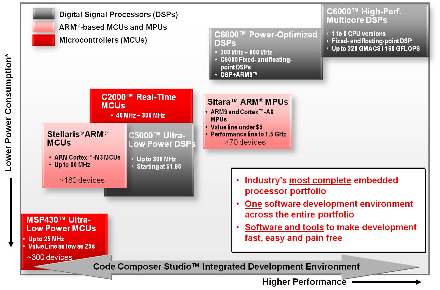
Figure 2 shows an alternate solution that allows you to build your own adaptor boards. It has multiple adaptor circuits on one board that split apart easily.
Enough about adaptors. It’s time for you to jump into the chapters on analog circuits. Each was written by an expert on TI’s application staff. Learn to enjoy the task of revisiting material you forgot right after the test. This will not be the first time you will relearn material, or in some cases learn it for the first time. It will be a career-long exercise as you grow with the technology.
This module reviews the concept and usage of the operational amplifier (op amp). It is aimed at the senior who is facing the task of choosing the right operational amplifier for their senior project. The module reviews the concepts of the op amp, how to read the data sheet (with keywords defined) and some suggestions on how to pick the right op amp for your project.
Operational amplifiers and other analog components
The op amp is perhaps the most versatile building block for analog circuits. With an op amp and a few passive components, you can make amplifiers of all sorts with inverting and noninverting gains. You can make integrators, differentiators, filters and voltage-level shifters. You can perform signal rectification, convert voltages to currents and vice versa. Applications information is widely available on Texas Instruments' website and across the Internet by searching with a few keywords.
Op Amps for Everyone is an excellent general reference. This section of the book will also briefly cover special amplifiers and related component types such as instrumentation amps, comparators and difference amps.
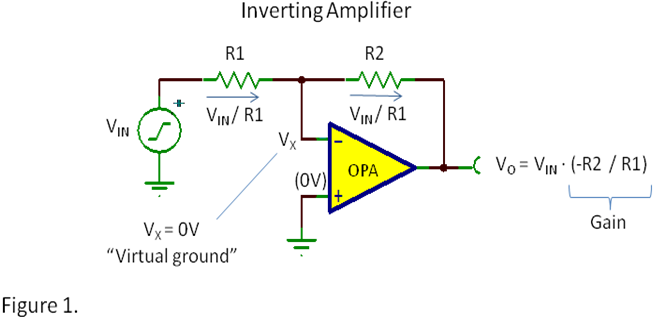
Let's start with some basics. If you recall the ideal op amp assumptions, the most important are infinite gain and infinite input impedance. The infinite gain assumption can be troubling. Think of it this way: When negative feedback is connected from output to input, the output seeks a voltage that creates 0 V between the two input terminals.
In Figure 1, the noninverting input voltage is clearly defined; it’s 0 V connected directly to ground. The voltage at the inverting input is determined by the voltage divider formed by R1 and R2. The op amp (with its feedback network) performs a balancing act, driving the output to a voltage that will make VX = 0 V. Any small deviation of VX away from zero will nudge the output in the direction to regain balance at 0 V. Some simple nodal equations involving VIN, VO and VX = 0 will yield the transfer function of this circuit.
The noninverting amplifier shown in Figure 2 is essentially the same circuit, with the input signal applied at a different node. The “input” side of R1 is now connected to ground and the noninverting input of the op amp is now the signal input terminal. Through feedback, the output seeks a voltage that causes the inverting input terminal voltage to be equal to VIN. Again, simple nodal analysis will yield the transfer function and gain. Note that the gain is different in this case with a “+1” term added.
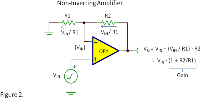
Although many complexities exist involving the nonideal behavior of op amps, understanding an application circuit always starts with a firm understanding of how the ideal circuit is meant to operate.
Finding your op amp
You’ve probably used a prescribed op amp in your labs, and your professors have designed assignments to suit the characteristics of the op amp you are using. When you need to select an op amp that meets the needs of your project, you will find that there are hundreds to choose from. Where do you start?
These key specifications are generally the most important selection criteria.
Operating voltage
Battery-operated projects generally use CMOS op amps operating from 5 V or less.
Often use CMOS op amps operating from 5 V or less.
Rail-to-rail op amps allow wider input and output voltage with limited supply voltage.
Higher voltages are often used for higher accuracy and special performance characteristics.
±15-V supplies are commonly used for instrumentation and measurement applications.
Dual (±) supplies are easier when accurate positive/negative signals are important.
Gain bandwidth (GBW)
Determines the signal bandwidth that you can achieve with a given closed-loop gain (G).
Maximum usable signal bandwidth = GBW / G.
Op amps meeting minimum requirements will use less power.
Op amps with unnecessarily high GBW (>50 MHz) may be more difficult to use.
Offset voltage (VOS or VIO)
The voltage between the two input terminals of the op amp (ideally zero).
Ranges from a few microvolts to a few millivolts.
Can be very important in processing accurate DC signal values.
Generally unimportant with AC signals such as audio.
Offset at the output is amplified by the closed-loop gain.
Input bias current (IB)
The current that flows in the input terminals of an op amp.
Ranges from picoamps to microamps.
CMOS and JFET op amps have the lowest IB.
Contributes to offset voltage by IB x Input Resistance.
Quiescent current (IQ)
The current drawn from the power supply with no load current.
Ranges from approximately 1 microamp to several milliamps.
Low IQ op amps are “slow” for low-bandwidth signals, battery-powered circuits.
Input common-mode voltage range and output voltage range
Among the most common difficulties users encounter are the limitations to input voltage range and output voltage swing. So-called “rail-to-rail” types have an input voltage range that extends to, or slightly beyond, the power supply rails. Those featuring a rail-to-rail output can swing close to the power supply rails. Rail-to-rail amplifiers are particularly useful in battery-operated circuits with low-voltage supplies.
Dual and quad versions, package types
Many op amps are available in single, dual and quad package versions. Dual and quad versions can save space (and money, if you are concerned about high-volume production). In a prototype development, however, single op amps make circuit board or prototyping easier.
There are many different package types. Newer, tiny surface-mount types may be difficult to handle in prototyping. Some new op amp types may not be available in the dual-inline (DIP) packages that are most convenient for prototyping.
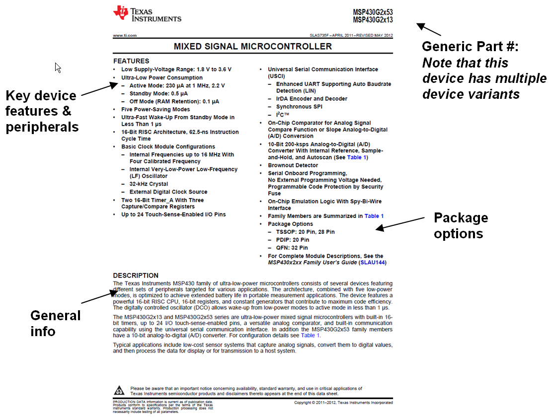
Reading the data sheet
An op amp data sheet can be a bit overwhelming – so much information for a device with only five pins. The summary of features and suggested applications on the front page tell you much about the intended uses of the device. You should have a clear idea of the key specifications that will drive your selection. Be aware of the conditions that apply to each parameter. Ones that apply to all parameters may be listed at the top of the specification table. Others for individual parameters may be listed in the “conditions” column. Understand that these conditions may be a formal way of defining how we measure a parameter, but may not preclude use in other conditions.
Typical performance graphs can tell you much about the basic nature of a device. This information is not generally assured by production testing and may vary from device to device. You will find some graphs, such as open-loop gain vs. frequency, in virtually every op amp data sheet. Other graphs will vary according to the behavior of that particular device and its expected uses.
The applications discussion can be quite helpful. It provides cautions and advice on how to best use the device. Application figures and diagrams can help explain best practices and how to get the most out of a particular op amp. Much of an op amp users' design knowledge comes from careful reading of data sheets.
Finding your op amp
Consider the op amps on the recommended list first. These devices cover a wide range of needs and have proven to be easy-to-use, capable performers. A variety of package types is available. DIP packages are easy for prototypes. Surface-mount types can be awkward for manual construction but do save space. You are not limited to these devices if you have special needs. There is a selection tool on our website that provides slider-bar tuning specifications. Go to http://www.ti.com/ and select Amplifiers and Linear.
Simulating with SPICE
You can download SPICE macromodels from http://www.ti.com/. They are found in the product folder for each device. Although you cannot simulate all components, such as data converters and controllers, simulating the critical analog portion of the signal chain does help solve basic problems and optimize your circuits. TI offers a free, easy-to-use SPICE simulation program with installed macromodels. Download it at http://www.ti.com/tina-ti.
Other amplifier types
There are a few other special amplifier types that deserve a brief introduction. You will find some of these devices in the TI recommended parts list.
Buffer amplifier. Increases the current output of an op amp to drive small speakers, motors, etc.
Difference amplifier. An op amp with four accurately matched resistors to measure voltage differences.
Comparators. Provide a binary output comparison of two analog voltages. Though some op amps can perform this function, comparators provide better features and performance.
Instrumentation amplifier. Three op amps and resistors to accurately acquire small-difference voltages in noisy environments.
Current shunt monitor. A special amplifier intended to measure current flowing in a shunt resistor, often used to measure current in a battery or power supply.
Programmable gain amplifier. Closed-loop gain is digitally controlled.
Current-feedback amplifier. A wide-bandwidth op amp similar to a standard op amp, with special restrictions on the feedback resistor values and configurations.
Voltage-controlled amplifier. Gain is controlled by an analog voltage signal.
You may also seek help on TI’s E2E Community forums. The op amps are handled in the Precision Amplifiers forum. Please read this short primer on submitting questions before posting to ensure prompt and efficient support.
This module is a brief overview of how ADCs and DACs function, how to read an ADC or DAC data sheet, and how to pick the right one for some sample applications. This module is one of many in a textbook designed for seniors considering the use of TI products in their senior project.
Technical overview
A data converter is the bridge between the real, physical world of analog signals like voltage or current, and the digital world of numbers represented by ones and zeros. An analog-to-digital converter (ADC) converts a voltage into a number; a digital-to-analog converter (DAC) converts a number into a voltage or current. An ADC might be used to measure a weight or the intensity of light, or allow an audio signal to be captured and stored as a digital file for playback in a media player. Converting that digital file back into sound would require a DAC; a DAC can also control a valve that affects the flow of chemicals into a chemical reaction, or the position of a cutting head on a system that makes mechanical parts.
ADCs
Figure 1 is a general representation of an ADC. An analog-to-digital converter can be represented by the three functional blocks shown here, regardless of architecture.
Every ADC consists of three functional blocks: a sampler, a quantizer and an encoder. In some architectures, some of the functions may actually be combined, but each function is there nonetheless.
The sampler is responsible for sampling the input signal at a certain time; it is implied that this function also “holds” the signal constant for the converter to operate on it during its conversion time.
The quantizer is responsible for measuring the input signal and determining an output code level that most closely represents the voltage of the analog input. It approximates the sampled voltage with a level from a fixed set of 2N possible voltage levels (where N is the number of bits of resolution), either via rounding or truncation.
The measurement of the input signal and creation of its corresponding output code are accomplished by comparing the input signal to a fixed reference voltage. The full-scale range (the maximum voltage that the converter can have on its input) is directly related to the reference voltage value. The minimum change in input voltage that the converter can detect is called the least significant bit (LSB) value. For example, if the full-scale range is the same as the 5-V reference voltage VREF, and the converter has 12 bits of resolution, the LSB would be given by Equation 1:
LSB = VREF/2N = 5 V/212 = 5 V/4096 = 1.22 mV (1)
You can generally achieve the best conversion accuracy by matching the input signal range closely to the converter's full-scale range, either through amplification before the ADC or by changing the reference voltage to adjust the full-scale range.
The encoder can turn the internal code used by the quantizer into a more usable code for a system (for example, turning a thermometer code into a twos complement code) or can simply format the code into a serial data stream for easy communication to a host processor.
Figure 2 is an example of how an ADC is connected in a basic data-acquisition system (based on the ADS8326). The reference voltage is supplied by the REF3240; both reference and signal inputs are buffered by op amps. The ADC is supplied power, a reference voltage and the input signal voltage by analog circuitry; the digital interface to a host microcontroller or DSP is often a simple serial interface. High-speed applications may require more involved signal drive circuitry; the data sheet for most ADCs usually shows the recommended circuitry needed around the ADC.
DACs
A digital-to-analog converter block diagram would be similar to Figure 1, viewed from right to left: the DAC accepts a digital input, which is then decoded into a form that the DAC circuitry can use. The quantizer then creates a voltage or current corresponding to the digital input value. The sampler is not always on the analog side because most DACs have a means to latch the digital value provided by the interface.
While ADCs generally accept only voltage inputs, the output of a DAC may be a voltage or a current. Figure 3 shows an example of a multiplying architecture, which usually has a current output, using an external op amp to convert the current to a voltage. Many DACs provide this conversion circuitry in the device itself. Like the ADC, the DAC requires a reference input and may require analog circuitry on its output. The digital interface is not shown. This DAC8811 provides the current output, which is converted to a voltage through the output op amp and an internal feedback resistor.

How to read a data converter data sheet
As with any electronic component, the data converter data sheet is an essential resource. When deciding on a converter to use for a design, much of what you need to know is usually prominently displayed on the first page of the data sheet. The most important parameters for a data converter are speed, resolution and accuracy.
Speed
For an ADC, speed refers to the time it takes to convert an analog input into a digital value – the actual specifications are acquisition time and conversion time, which when combined limit how fast the ADC can output a conversion result. This can also be expressed as throughput, which is usually shown as the maximum sampling frequency.
For a DAC, the limiting factor on speed is usually the settling time, which is the time it takes for the output to settle to a new value from a previous value within a specified error band. A 1-µs settling time implies that the converter may be suitable for updating its output at a rate up to 1 MHz.
Resolution
As described previously and with the example shown in Equation 1, resolution refers to the either the number of bits (N) that the converter has as its input or output, the number of counts or codes (which is simply 2N), or the value of the least-significant bit in volts or amps. Higher resolution means that the converter can discriminate between smaller changes on the input signal or provide more precise control over an output signal.
Accuracy
Many people confuse resolution with accuracy. Just because you have a converter with 16 bits of resolution doesn’t mean you always have 16 bits (or 15 ppm) of accuracy. Recall that a data converter requires a reference, and accuracy is the degree to which the result conforms to the correct value measured against a standard or reference. If you put exactly 1 V into an ADC and could resolve exactly that value with 16 bits, but the ADC tells you that it’s 1.2 V, that’s only 20 percent accuracy – a far cry from 15 ppm.
At a system level, the accuracy of the reference voltage will be one of the primary factors in the overall accuracy of the system. But the data converter itself contributes some errors. Some data converters will express an overall accuracy specification – often called total unadjusted error – but it is more common to see specifications for offset error, gain error and linearity.
The ideal transfer function for a data converter is shown in Figure 4, as a blue line. It appears as a staircase because the quantizer can only represent a range of voltages with a single code. The location of the transition point from one code to another is key to describing the converter's accuracy.
Offset error is the difference between the actual transition point and the ideal transition point – resulting in a translation of the transfer function left or right. Although this error is measured around a near-zero voltage input or output, the error continues throughout the entire transfer function from zero to a full-scale (FS) voltage. Consequently, the offset error near zero is the same as the offset error with a near FS voltage.