This module introduces the embedded processor section of the senior project textbook.
Introduction
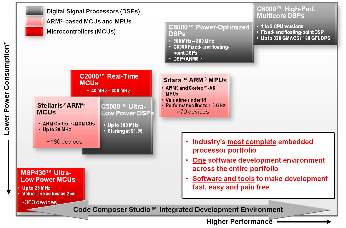
Texas Instruments has a wide range of embedded processors available to design into your project. Your choices include virtually everything from very low cost to very high performance, as well as a new performance metric called power dissipation. Figure 1 gives a quick overview of our embedded processor product line.
You should be able to complete your project using one of the following product families:
The MSP430™ ultra-low-power system microcontroller family.
C2000™ microcontrollers used in control systems.
ARM devices (specifically the M3/4 microcontrollers).
The C5000™ low-power signal-processing solution.
TI's other embedded processors fall beyond the scope of a typical two-semester senior project. We will spend time on the families listed here in the following chapters, focusing on those embedded processors that will best fit your project.
Remember, the best way to take advantage of an embedded processor is to use an evaluation module (EVM). You can find these listed for various processors on www.ti.com.
This module gives a brief overview of the MSP430™ microcontroller, how to read a data sheet for an MSP430™ microcontroller, and how to pick the right one for some sample applications. This module is one of many in a textbook designed to help seniors select TI products for use in their senior project.
MSP430™ microcontrollers
MSP430™ microcontrollers (MCUs) from Texas Instruments are 16-bit, RISC-based, mixed-signal processors designed specifically for ultra-low power. MSP430 MCUs have the right mix of analog and digital integrated intelligent peripherals, ease of use, low cost and lowest power consumption for thousands of applications ranging from simple sensor designs to complex electricity meters.
To get a better idea of what the MSP430 MCU is and how you can use it to solve a system design need or application problem, let’s take a look at a typical block diagram for a device. Figure 1 is the device block diagram for the MSP430G2553, one of the MSP430 Value Line devices.
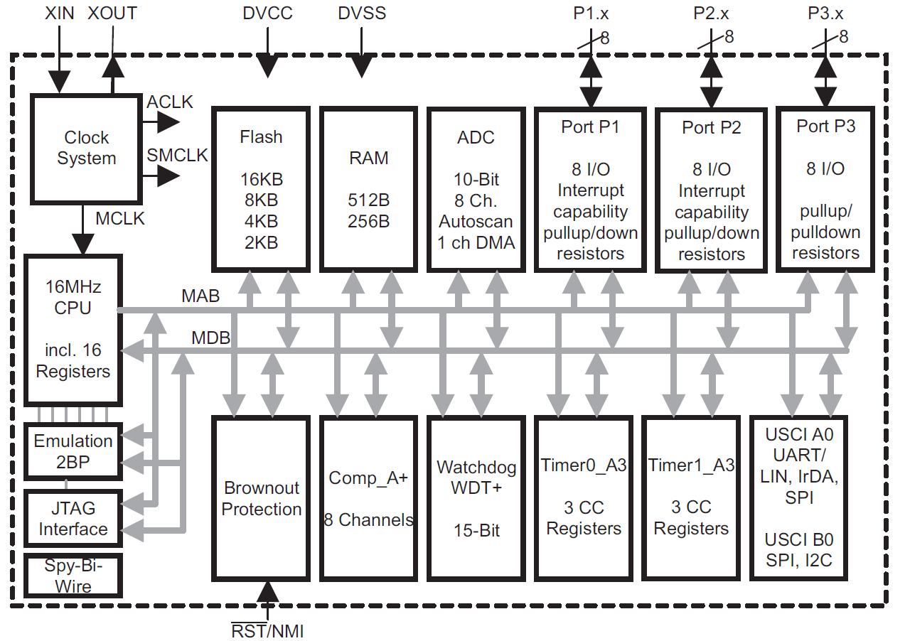
The purpose of the block diagram is to provide a high-level reference of the integration and feature set found in a given device. You can find the block diagram for any MSP430 MCU in the data sheets at www.msp430.com.
The block diagram contains key features of the device that can help you quickly identify if an MSP430 MCU is a fit for a given application need. There are a few features you will need to consider:
Integrated memory:
Includes both volatile (RAM) and nonvolatile (flash) sizes.
When multiple values are listed, it shows which device memory size variants are available with the same peripherals.
General-purpose I/O pins:
The MSP430G2553 has up to 24 I/Os available: eight Port1 (P1), eight P2 and eight P3 I/Os.
Package-dependent: Check the pinout for the total number.
All pins have configurable integrated pullup or pulldown resistors.
P1 and P2 I/Os when inputs can provide an interrupt to the CPU.
CPU and emulation capabilities:
16 MHz is the maximum CPU clock speed for the MSP430G2553.
Integrated emulation for the MSP430G2553 has two hardware breakpoints (2BP) for use when debugging.
Simplified clock system:
One external clock source on XIN/XOUT can be sourced.
The internal clock tree provides three clock tree branches.
Digital and analog peripheral mix. The MSP430G2553 device includes:
10-bit, eight-channel analog-to-digital converter (ADC) with internal voltage reference for voltage measurement (sensors, power rails, etc).
Comp_A+: eight-channel analog comparator with internal voltage reference for simple measurements or voltage threshold detection.
WDT+: watchdog timer for resetting the CPU in case of timeout (can also be used as a simple interval timer generating an interrupt).
Timer0,1_A3: two 16-bit general-purpose timers, each with three capture-compare (CC) I/Os.
USCI (A0/B0): universal serial communication interface module capable of providing standard UART, SPI and I2C communication protocols used to interface with external digital devices (sensors, data converters, radio ICs).
Figure 2 is the corresponding pinout also found in each device data sheet for the MSP430G2553. Here you can see exactly how peripheral functions are mapped onto the multiplexed I/Os of the device. Each I/O pin can be configured in software to provide the desired pin function for a given I/O based on its internal connectivity.
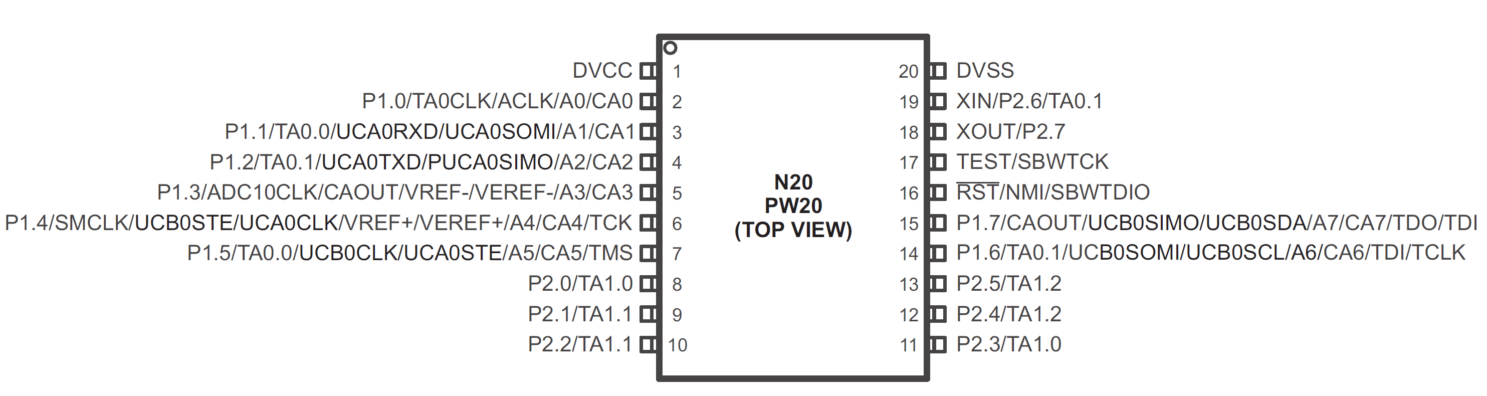
Figure 2 also shows the necessary power-supply connections (DVCC, DVSS), programmer/debugging tool connections (SBWTCK, SBWTDIO), and general I/O and peripheral connections (P3.1, TA1.0, CA2, UCB0SDA). When beginning any design with the MSP430 MCU, reviewing the given device’s block diagram and package pinout can provide a great guide to what is possible, as well as any constraints (such as memory size or pinout limitations).
Connecting the MSP430 MCU in any system is, in most cases, very straightforward. The first consideration should be the power-supply requirements. Most MSP430 devices operate at 1.8 V to 3.6 V, so a typical 3-V supply will work great. Connecting the JTAG to support device memory programming and debugging is also important. For MSP430G2xxx devices, there are two possibilities: standard four-wire JTAG or MSP430 MCU-specific Spy-Bi-Wire (SBW, or two-wire JTAG). Both interfaces are acceptable for programming and debugging application code. The main advantage of the four-wire mode is speed. The main advantage of the two-wire SBW mode is reduced pin-connection requirements.
Figure 3 is an example schematic thatshows the baseline connections for the MSP430G2553, as well as some examples of other connections that can be made to the I/Os and integrated peripherals.

Figure 3 shows the connections of the MSP430G2553 in a typical sensor interface application. In this example, the MSP430G2553's integrated ADC10 is used to measure an analog signal via a thermistor that changes resistance as temperature increases or decreases, and also interfaces using an I2C bus from the USCI module to an external humidity sensor. In addition, a 32.768-kHz watch crystal keeps accurate timing; two switches, along with one PWM-controlled LED, provide a simple user interface. To save power from the 3-V coin cell battery, when not in use the humidity sensor and thermistor ladder can be powered off using a general-purpose I/O (P2.5) and the internal voltage reference (VREF+), respectively.
Now that we've covered the basics and how to understand the capabilities of a given MSP430 device, let’s look more closely at the documentation and how to use it most effectively. MSP430 device documentation can be broken up into three main categories:
Device-specific data sheet (e.g., MSP430G2553 data sheet.) Here, you will find anything device-specific: pinouts, block diagrams, absolute operating conditions (supply voltage and operating temperature ranges), electrical parameters and performance tolerances (power consumption, ADC accuracy, and internal clock minimum and maximum frequencies).
Device family user’s guide (e.g., MSP430x2xx family user's guide). This document contains information applicable to all devices in a family: peripheral detailed descriptions, register and bit function definitions, CPU and instruction set, power mode definitions and settings. Some peripherals included in the user’s guide will not be present in a given device, as it is intended to cover all peripherals within a given family.
Device-specific errata sheet (e.g., MSP430G2553 device errata sheet). The errata sheet is a critical document that lists any device bugs that can affect a given use-case along with potential workarounds. Errata can vary by device as well as device revisions.
You can find these documents, as well as additional reference material such as application notes, example code and development tool documentation, by navigating to the device-specific product folder (e.g., MSP430G2553 product folder). Here, you can find the latest information as well as links to all pertinent documentation and software to aid your design efforts.
Arguably, the most valuable document is the device-specific data sheet. We have already looked at two core aspects (pinout and block diagram), but let’s dive a bit deeper into the information provided. The front page of the data sheet is designed to highlight all of the key aspects of the device organized into bulleted lists (Figure 4). It is comprehensive, showing typical power consumption, clock system capabilities, peripheral mix and package options.
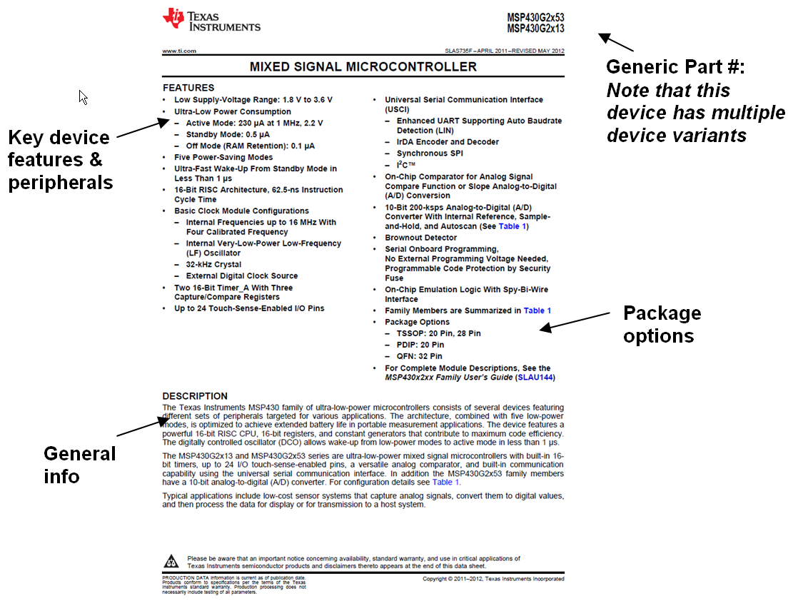
This information is a great start, but is targeted as more of a marketing message than a reference. Going beyond the first page is critical to fully assess the given device’s capabilities and its limitations. Looking beyond the first page begins to yield the information needed to really design a system with the MSP430 MCU. This begins with the available options for the device and variants. For example, there are 40 device and orderable part number variants for the MSP430G2553 device. These variants provide different mixes of flash or RAM, peripherals available, number of I/Os supported, and package options such as DIP or surface-mount options.
While all information in a data sheet should be considered important, we recommend focusing on these areas when reviewing a data sheet for a specific MSP430 MCU:
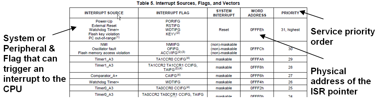
Supported interrupt sources, corresponding flags and priority (Figure 5).
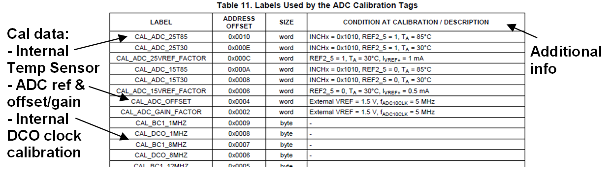
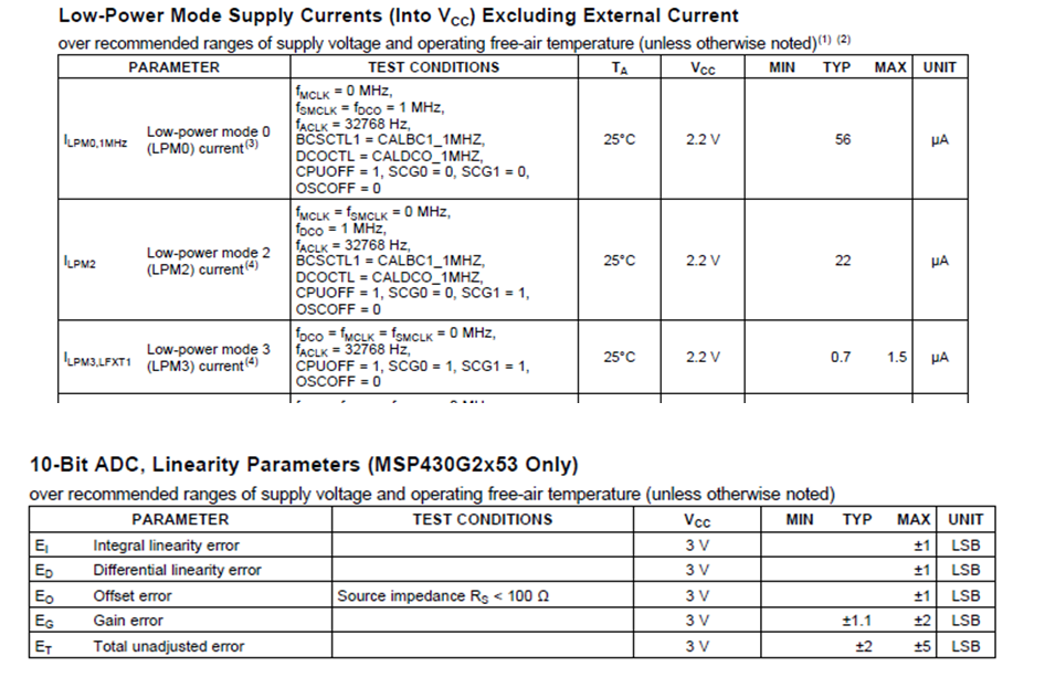
Calibration data such as internal clock defaults and ADC offset/gain settings (Figure 6).
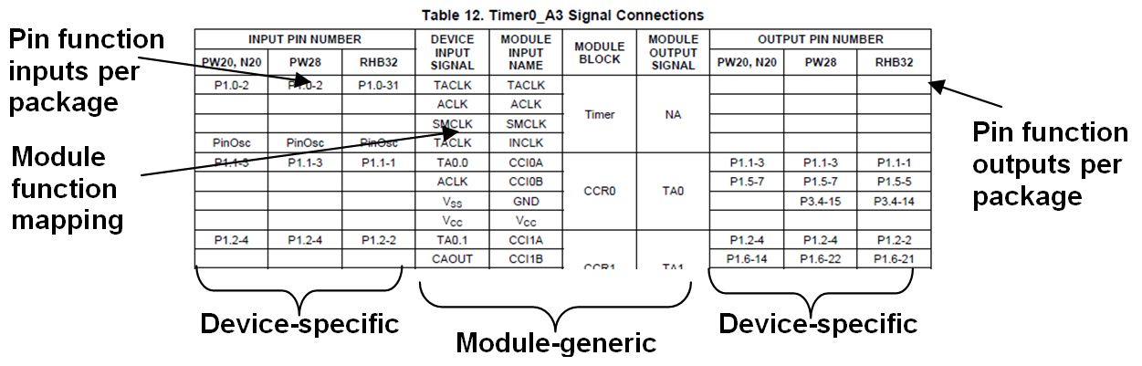
Timer functions and pinouts for each capture-compare I/O (Figure 7).
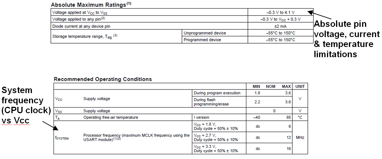
Absolute maximum ratings and recommended operating conditions, including voltage and temperature, as well as CPU clock speeds vs. Vcc (Figure 8).
Performance specifications for power consumption, analog accuracy, clock tolerances, etc. (Current consumption and ADC performance excerpts shown in Figure 9).
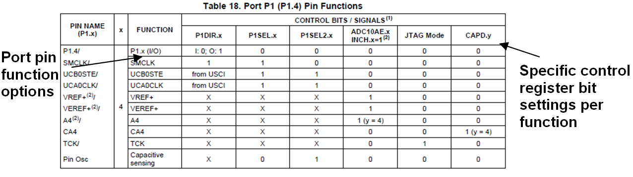
Port schematics and pin function tables that detail exactly how to select a given multiplexed function on a given pin using the I/O control registers (Figure 10).
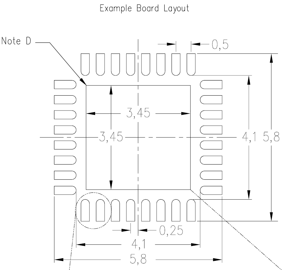
Package information providing package tolerances, useful when creating device footprints in schematic/PCB CAD tools (Figure 11).
Now that we have reviewed the MSP430 device documentation and where to find information about what a device can do, let’s walk through the process of actually selecting the part that best suits a given design need.
Let’s start by answering the questions below:
| 1. “What problem am I trying to solve?” This is fundamental. Until you understand this, nothing else can happen. Knowing what problem you face at a system level allows you to identify how the MCU's features can help you solve that problem most efficiently. |
Do analog signals need to be measured, such as a voltage from a strain gauge or an output from a potentiometer? If so, perhaps an integrated ADC is of value. If a simple analog threshold is all you need, an integrated comparator will likely do the trick.
What is the user interface? Switches likely translate into simple digital interrupt inputs, while displays may require a communication bus such as SPI in order to refresh the data displayed.
Are time-sensitive signals needed off-chip? Perhaps you need a PWM signal to control a motor’s speed or LED brightness.
What are the other devices or circuits that the MCU needs to interface with? Identifying potential analog inputs, logic-level digital I/O signals, or communication interfaces such as I2C or UART will all help you find the right MCU to fit the application need.
| 2. “How many 'things' need to be input into the device or driven from the device [as outputs])?” Determining this at a block level for the system, and then at a more detailed MCU pinout level, will clarify exactly how many I/O pins you will need. |
| 3. “What are my power-supply requirements/limitations?” This is important, as the MCU supply may impact the overall system design. For example, if powered from a 9-V battery, the MSP430 MCU will need a regulator to bring its supply to within the 1.8- to 3.6-V range. |
| 4. “How much memory will my application need?” This is not always obvious, as the software may not yet be written. But if you plan on using existing code, or modifying code already written, you can get an idea of what a given function in software might require in terms of program and data-memory needs. And when you need certain algorithms such as fast Fourier transform or filtering, you can often estimate RAM requirements before ever selecting the device by simulating the functions on a PC. |
| 5. “Are any ‘special’ features needed?” For example, do you need a USB interface to a PC? Or a high-resolution ADC (>12 bits) to get a certain system performance? Consider looking for MCUs that offer such features integrated to minimize the system-level design effort and complexity required. |
| 6. “Are there any physical design or assembly constraints (package size, pin spacing, PCB or assembly capability)?” Often, the box the final system must fit into is a factor. This can have big implications on package requirements, pin-count limits and PCB design complexity/cost. Also consider testing a final system – the more dense a design or package is with respect to PCB routing, the more challenging it is to assemble and debug. DIPs are easiest, with BGAs being quite challenging. |
Numerous devices available in the MSP430 family portfolio can meet the given system requirements uncovered in these questions. We've listed a few in Table 1, with their own unique feature sets. A key driver in listing these specific parts is their ease of use. They are available in DIP packages and are supported by a flexible and scalable development tool that can accelerate prototyping of a given application.
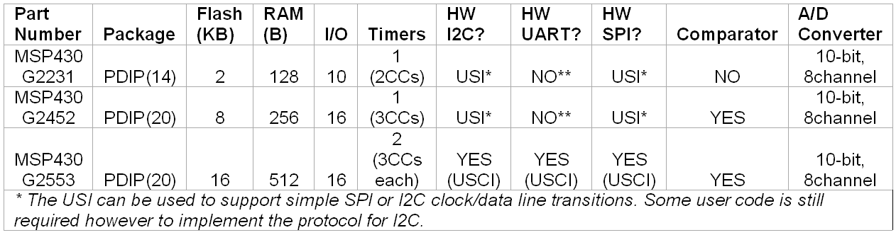
Table 1. Three MSP430 devices with typical characteristics.
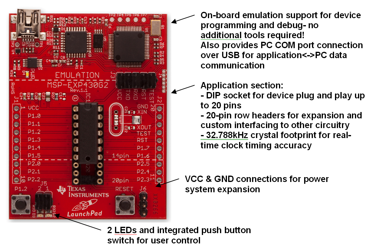
Each of the devices can be used with the MSP430 MCU LaunchPad to provide an easy, intuitive and out-of-the-box development experience (Figure 12).
Solving any design challenge begins by understanding the problem and any constraints that the system may have. Once you have established a clear picture of the problem you need to solve, finding the ideal way to solve that problem – using an MCU – can be straightforward if you understand the capabilities that MCUs offer. Being able to navigate the MSP430 family, its feature set, and the available devices and development tools are keys to success in meeting such a system design challenge.
This module gives an overview of the C2000™ family of microcontrollers from Texas Instruments. It includes an overview of the architecture, helpful hints on how to read data sheets and a quick guide to pick the right device for a project. This module is part of a collection of modules aimed at seniors in college who are starting to work on their senior project.
The TMS320C2000™ family of microcontrollers (also known as the C2000™ family) is a product line aimed at high-performance control applications such as motor control, digital power supplies, lighting, renewable energy and smart grid. This family is made up of several subfamilies, with names like:
C24xx: A 16-bit microcontroller that evolved from the TMS320C2x family of digital signal processors.
C27xx: A 16-bit microcontroller that is no longer recommended for new designs, so we will not cover it here.
C28xx: The current family of devices that are 32-bit fixed or floating point, with a robust set of peripherals and I/Os to match the exhaustable need for performance in control applications.
The C28xx family is further divided into:
Delfino™ floating-point MCUs:
Performance: 100-300 MHz.
Memory:
Up to 512-kB flash.
Up to 516-kB SRAM.
Key peripherals: ADC, PWM, QEP, DMA, SPI, UART, I2C, CAN, EMIF.
Piccolo™ fixed-point MCUs:
Performance: 40-80 MHz.
Memory:
16 to 128-kB flash.
6- to 100-kB SRAM.
Key peripherals: ADC, PWM, QEP, DMA, SPI, UART, I2C, CAN, USB.
Concerto™ C28x core plus M4 ARM processor:
Performance:
Dual core:
Up to 150 MHz 28x CPU.
Up to 100 MHz M3 CPU.
Floating-point unit.
VCU accelerator.
Memory:
16- to 128-kB flash.
6- to 100-kB SRAM.
Key peripherals: ADC, PWM, QEP, DMA, SPI, UART, I2C, CAN, USB, EMIF, EMAC.
Let's use the Piccolo MCU to overview the architecture of the family, specifically the TMS320F28027. I have chosen this device because it's the one used in the C2000 LaunchPad™ development tool (shown in Figure 1).
Architecture
A quick look at the CPU:
High-efficiency 32-bit CPU:
Clock frequencies of 40, 50 and 60 MHz.
16-bit and 32-bit hardware multiply and accumulate (MAC) operations, including a dual 16-bit MAC capability.