chemically non-resistive glues. It leads to rapid glue destruction and appearance of leakages
what can not be accepted due to safety reasons. The unique feature of developed by us
microsensor was application of thin silicon wall separating fluidic microchannel from
microchannel with optical fibers. It is well known that thin (below 20 m) silicon layer is
transparent for near-infrared light (Fig. 27). Thus, physical separation with simultaneous
NIR transmittance was obtained.
The technology of novel optical microsensor utilized standard microengineering techniques.
The fluidic channel and alignment grooves were etched by deep reaction ion etching (DRIE)
in 380 m thick, double-side polished, (100)-oriented silicon substrate. DRIE process has
been optimized to obtain the vertical side-walls of the channel. Two type of microchannels
were formed. The first type was microfluidical channels, the second one – microchannels for
positioning of optical fibers. After DRE etching these two types of channels were separated
by 20 m thick silicon wall with perpendicular walls. Photolithographically patterned 100
nm Al mask layer was used to form fluidic inlet/outlet holes form back side of the wafer.
The silicon substrate was thermally wet oxidized again to obtain 0.3 m SiO2 isolation layer
serving as chemically resistive layer. Next, the silicon substrate was anodically bonded
(450oC, 1.5 kV) to a Borofloat® 33 glass (Schott, Germany).
High quality bonding process was required to ensure the leakproofness of the channel.
Finally, the optical fibers equipped with SMA connections were positioned in the alignment


Microsensors for Microreaction and Lab-on-a-chip Applications
131
grooves and immobilized by a droplet of UV-curable optical glue UVO-114 (Epo-Tec,
Germany) (Fig. 28).
12000
11000
13 um
21 um
10000
25 um
9000
]
32 um
8000
37 um
ce [au
7000
49 um
6000
ittan
5000
smn 4000
raT 3000
2000
1000
0
550
600
650
700
750
800
850
900
950
Wavelength [nm]
Fig. 27. Transmittance of thin silicon membrane (thickness from 13 m to 49 m)
a) b)
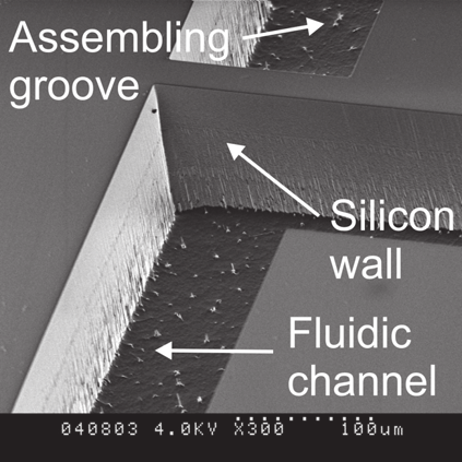
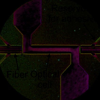
Fig. 28. NIR spectrophotometric microfluidical sensor: a) schematic top view and cross-
section of the microsensor, b) SEM picture of the thin silicon wall separating microfludical
channels for liquids and optical fiber positioning after DRIE etching (upper picture) and
optical microscope picture of the measurement cell with assembled optical fibers (lower
picture).
132
Microsensors
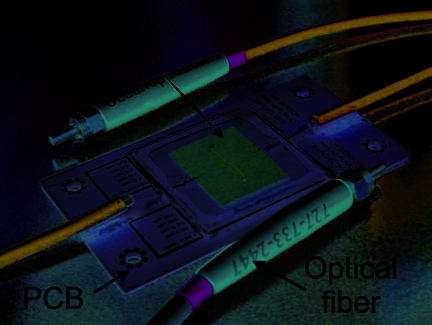
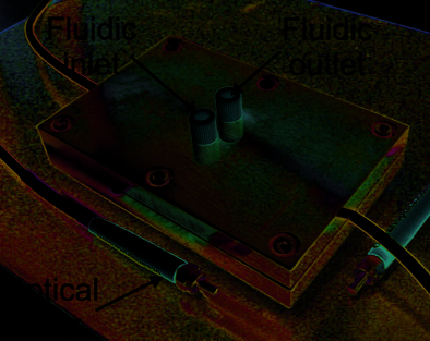
Assembled microfluidical sensor was placed on a PCB carrier and mounted in a metal
package with tight and chemically resistive standardized fluidic connections (UpChurch,
USA) (Fig. 29a, b).
a)
b)
c)
Fig. 29. NIR spectrophotometric microfluidical sensor: a) the chip mounted on a PCB ensuring
proper mechanical stiffness and robustness, b) the chip mounted in a metal package ready
with fluidic connections, c) scheme of the measurement set-up for NIR spectrophotometric
characterization of aggressive liquids by microfluidical silicon-glass sensor
The NIR system was composed of a halogen light source, a silicon-glass corrosion resistant
optical cell, and a NIR mini-spectrometer C9406 (Hamamatsu, Japan) (Fig. 29c). The cell
with optical path length of 5 mm had detection volume of only 90 nL. The system was
controlled by a notebook with suitable software.
The miniature spectrometric system has been tested experimentally by the measuring of
NIR spectra of several samples including highly corrosive reactants of nitration reaction.
The detection unit worked correctly at wide range of flow rates (0-300 ml/h) what
confirmed its mechanical robustness. The 24 h-long test with the measurement cell filled
with pure nitric acid followed by sulphuric acid showed corrosion resistance of the
detection chip. The spectra of pure nitric and sulphuric acids as well as theirs mixtures with
deionized water were successfully obtained (Fig. 30).
In further tests it has been clearly shown that the microsensor recognizes properly different
diesel oils and furnace oil as well as gasoline. Concentration of ETOH in Porto red wine has
been very well examined. Experimental results confirm the full applicability of the
miniature corrosion resistant NIR spectrometric system for use in wide range of
applications, e.g. mTAS, microreaction technology, biomedical/medical measurements. The

Microsensors for Microreaction and Lab-on-a-chip Applications
133
maximal wavelength is limited by the properties of array detector applied in miniature
Hamamatsu spectrometer. The use of longer NIR wavelengths (up to 2500 nm) is not limited
by the micromachined detection cell.
a)
b)
Fig. 30. The spectra of concentrated pure sulphuric (a) and nitric (b) acids as well as theirs
mixtures with deionized water, calibration curves describing absorbance versus DI water
content are shown below spectra
4.2 Absorbance VIS detector for optical characterization of living oocytes and
embryos
Optical characterization of living reproductive cells is an important issue in assisted
reproduction techniques. The major goal of these techniques is improvement of in vitro
fertilization process towards more successful breeding of farm animals. It is well known that
only 5-10% of in vitro fertilized oocytes are viable enough to reach full development
competence embryo stage. Assessment of development competence of oocytes and embryos
based on lab-on-a-chip system with analyze of the spectral characteristic of the cells, is an
important element in research on assisted reproductive technologies. Typical diameter of
porcine or bovine oocytes is in 100 m - 150 m range, similar dimensions are characteristic
for embryos. Due to size and volume incompatibility, spectrophotometric characterization
of these cells is impossible in typical measurement cuvette with 10 mm-long optical path
and at least a few hundreds microlitres volume. On the other hand, miniaturized
spectrometers and light sources co-working with optical fibers as light guiders to and from
characterized object are available now. What more, lab-on-a-chip techniques enables
134
Microsensors
fabrication of microchannels with diameter similar to the size of oocytes/embryos and
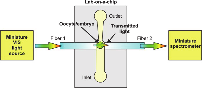
optical fibres (Szczepanska at al., 2009) (Fig. 31a).
a) b)
Fig. 31. Scheme of an idea of the spectrophotometric characterization of single oocyte or
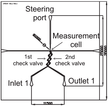
embryo in a lab-on-a-chip (a) and layout of the real lab-on-a-chip, the dimensions are in m
Lab-on-a-chip contains measurement cell, net of microchannels and passive valves for steering
of fluid and oocyte/embryo flow, and inlet/outlet holes for biological material
loading/unloading as well as a steering port for fluid flow management (Fig. 31b). The
biological material is introduced into the measurement cell by inlet 1, than passes through set
of passive Tesla’s valves (1st check valve). Next, characterized cell flows into the measurement
cell by sucking of the fluid by a pipette connected to the steering port of the chip. Topology of
the measurement cell ensures mechanical immobilization of the cell between two optical
fibers. After characterization, the cell is flushed back to the outlet 1 by passing through the
second set of Tesla’s valves (2nd check valve). Developed configuration enables steering of the
fluid flow with examined biological material transport with separation of the inlet and outlet.
The fluidic microchannels and microchannels for optical fibers (all 140 m deep) were
etched simultaneously in DRIE process in the 380 m - thick monocrystalline silicon wafer
(Fig. 32a). After etching, 0,3 m - thick thermal silicon oxide is was formed to passivate
chemically surface of the chip. Next, the wafer was anodically bonded (4500C, 1,5 kV) to a
borosilicate glass (Borofloat Schott, Germany) with previously mechanically drilled inlet
and outlet via - holes. Following, optical fibers with outer diameter of 120 m and 100 m
core (Ocean Optics, USA) were mounted. Fronts of the fibers were perfectly aligned each to
other thanks to high precision of DRIE etching. Fibers were aligned to the edge of
microfluidical channel, ensuring immobilization of the oocyte without its mechanical
destruction (Fig. 32c). Fibers were fixed by the use of UV NOA 61 epoxy hard glue
(Thorlabs, Sweden). Off-chip ends of both fibers were finished with standard SMA 905
connectors compatible with optical connections of the lamp and the spectrometer. Finally,
the chip was positioned in a metal package ensuring stable operation during
oocyte/embryo management within the chip (Fig. 32b).
The single oocyte/embryo was introduced into lab-on-a-chip by manual pipeting followed
by transport of the cell into the measurement cell thanks to capillary forces. After short
measurement (circa 5 seconds) of the optical spectra, the biological material was carefully
flushed-back to the outlet by applying pressure into the steering port. Then the cell was
captured to a sterile transporting container for further treatment.

Microsensors for Microreaction and Lab-on-a-chip Applications
135
The measurement set-up consisted of VIS/NIR light source (a halogen lamp by
OceanOptics, USA), developed by us lab-on-a-chip, miniature spectrometer (Ocean Optics,
USA) and a personal computer with specialized software (this set-up was similar to
presented on figure 31).
a) b) c)
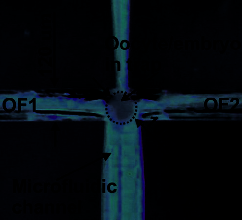
Fig. 32. Lab-on-a-chip for VIS spectrophotometric characterization of oocytes/embryos: a)
enlarged view of the silicon chip after DRIE etching - microchannels for optical fibers,
measurement cell in the center and Tesla’s valves set are visible, b) packaged lab-on-a-chip
ready to work in comparison to Polish 2 zloty coin, c) view of the measurement cell with
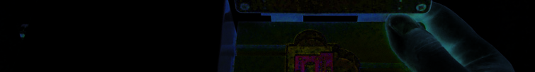
trapped cell (OF1 and OF2 are optical fibers no 1 and 2)
Totally, over five hundreds of porcine and bovine oocytes, as well as almost one hundred of
bovine embryos were optically characterized by novel methodology and lab-on-a-chip.
Differentiation of collected spectral characteristics of the cells coming from different
classification groups (for example ovarian follicle size or morphological properties) has been
observed (Fig. 33). On the base of collected data, set of numerical values, describing
subjectively optical properties of examined cell, has been proposed: absorbance level for
specific wavelength, absorbance ratio for two wavelengths and wavelength position of the
absorbance maxima in VIS region.
a) b)
Fig. 33. Example of absorbance spectra obtained for: a) porcine oocytes coming from
different sizes of ovarian follicles, b) bovine oocytes for different morphological classes
136
Microsensors
Further experiments confirmed non-destructive nature of spectrophotometric oocyte
characterization. Successful in vitro bovine oocyte fertilization after lab-on-a-chip
examination has been achieved. This result opens a way towards oocytes selection for
artificial fertilization of farm animals oocytes as well as quality assessment of embryos prior
to the implantation.
4.3 Fluorometric detector
Labs-on-a-chip dedicated for fluorescence detection of analyte must enable introduction of
the fluorescence inducing light and collection of the fluorescence light from an area of
interest within the chip. Usually, the chips are whole made of visible light-transparent
materials – like glass, PDMS, SU-8, COC or other polymers – or only a top cover of the chip
is made of glass, PDMS or other light-transparent materials. Most of the chips are design to
co-work with typical apparatus applied for fluorescence induction and readout –
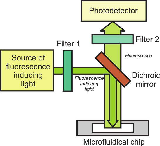
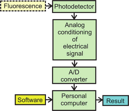
epifluorescence microscope (Fig. 34). In this devices, light, usually from arc lamp, light
emitting diode (LED) or laser, is restricted to a narrow range of wavelengths that can
effectively excitate a fluorochrome and be strongly filtered by the detection channel. The
narrow wavelength range is ensured by one or more interference filters and a dichroic
mirror. Fluorescence light emitted by the fluorochrome is collected by the microscope
objective and guided to a photodetector, passing through filters and dichroic mirror to
exclude the excitation light. Common detectors include photomultipliers tube (PMT),
semiconductor photodiodes and cooled charge coupled devices (CCD) as sensing matrix in
video cameras or lines in spectrometers. Light sources and photodetectors co-work with
analog conditioning electronics. The electronic circuits amplify electrical signal with
simultaneous reduction of noises. Most of the conditioning electronics is realized by the use
of analog circuits. These circuits must ensure high signal to noise ratio (SNR) before the
analog signal is digitalized. Therefore, configuration of these analog circuits is sophisticated
and only the highest quality elements can be used.
a) b)
Fig. 34. Fluorescence detection by epifluorescence microscope: a ) scheme of the methods, b)
path of fluorescence signal conditioning
Although, fluorescence detection is widely used for many years, the configuration of
detection apparatus co-working with labs-on-a-chip is based on solutions developed over 20
Microsensors for Microreaction and Lab-on-a-chip Applications
137
years ago. Therefore, rapid development of the LOCs must be followed by development of
novel methodologies and technical solutions surrounding the chips and leading towards
successful application of the microfludical chips in the point-of-care devices.
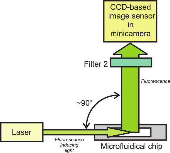
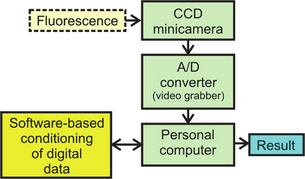
In the novel concept of the optical instrumentation for fluorescence induction and readout,
application of recent developments in optoelectronics and informatics is involved (Fig. 35).
a) b)
Fig. 35. Fluorescence detection by image sensor and orthogonal configuration of
induction/detection channels microscope: a ) scheme of the methods, b) path of fluorescence
signal conditioning
The fluorescence light is induced by a miniature semiconductor laser. Narrow- spectrum of
the laser light eliminates application of emission filter. Collimated laser light is introduced -
by edge coupling to a light guiding side wall of the chip - directly into detection area of the
chip. The view of the detection area containing fluorescence signal is collected by a CCD
image sensor being a part of low-cost minicamera module. The detection unit is positioned
perpendicularly in relation to the surface of the chip and laser beam. It enables geometrical
separation of the laser excitation light and fluorescence signal without application of
dichroic mirror, what significantly simplifies the optical part of the detection unit.
Therefore, detection unit consist of only one optical filter passing through the fluorescence
light and a miniature black/white CCD camera with the objective. The non-conditioned
analog output signal from the minicamera is digitalized by one-channel low-cost frame
grabber connected to a personal computer (PC). PC stores images in a memory and
specialized software carries out analyze of the captured images to give information on
fluorescence intensity. Thus, digital conditioning of the fluorescence signal by the software-
base image analyze in spite of analog conditioning is applied in the novel concept. Unique
feature of the novel methodology is possible re-analyze of the images which are stored in
the computer memory. It is not available in typical instrumentation with “non-imagining”
photodetectors (PMT or photodiode) when an operator has no chance for the second analye
of carried out experiment.
Novel fluorescence detection methodology and instrumentation co-working with various
labs-ona-chip have been successfully applied in many life-science applications –a portable
real-time PCR DNA analyzer, a novel portable cocaine detector, a miniature microcytometer
for optical characterization of biosamples or on-chip DNA gel electrophoresis.


138
Microsensors
One of the most interesting and promising applications of LOCs and presented here
fluorescence methodology is portable device for detection of food borne pathogens –
Campyloabcer j. and Salmonella spp. by specific amplification of bacteria’s extracted DNA with real-time detection of fluorescence – real-time polymerase chain reaction (PCR). This
instrumentation has been developed under European project OPTOLABCARD (Ruano-
Lopez at al., 2009). The device consists of a disposable real-time PCR chip, a docking station
with a specialized chip holder (Fig. 36) and electronics circuits and specialized software for
fluorescence signal detection and PCR process temperature profile management.
a)
b)
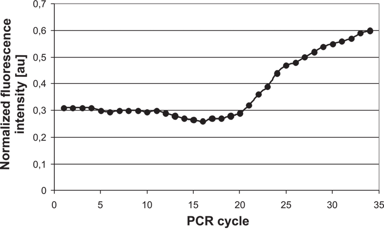
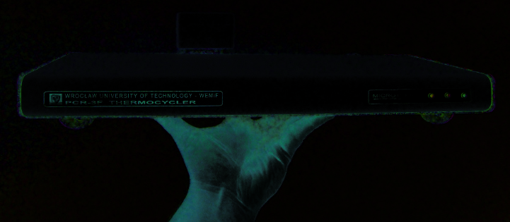
Fig. 36. Portable real-time PCR DNA analyzer utilizing disposable chips: a) view of the
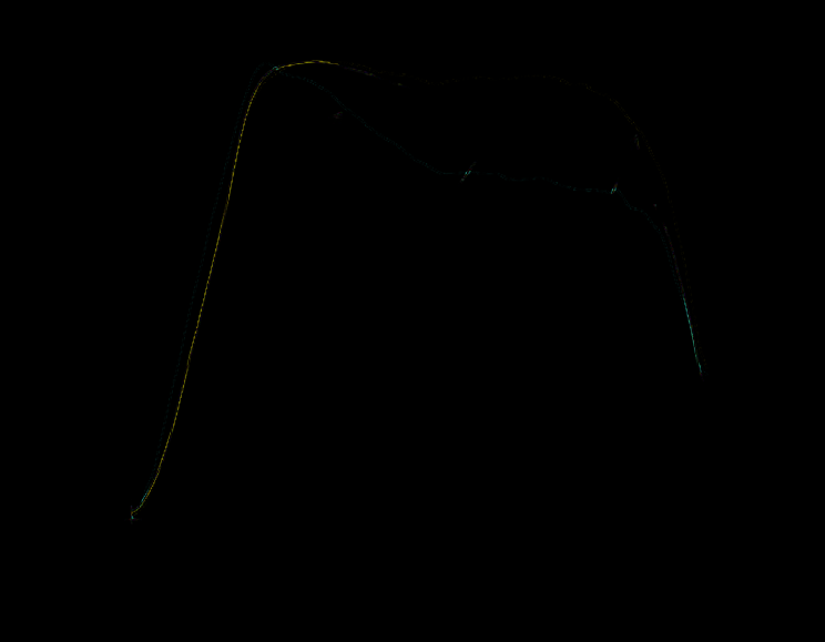
docking station with mounted chip holder, b) typical real-time PCR S-curve of Campylobacter
j. DNA amplification and detection
The disposable glass/SU-8 chip (1 x 1 cm2) with integrated heater and temperature sensor is
placed in a plastic chip holder (2.8 x 2.8 . 0.5 cm3) with integrated electrical contacts to the
chip and some electronics for temperature management. The chip holder has miniature
electrical connection to a specialized PCR temperature controller connected to PC. The
holder with ready to use chip is positioned in the docking station (15 x 5 x 7 cm3) in the way
ensuring laser light introduction into PCR microchamber and fluorescence light collection.
The pre-validation tests of LOC-based system for detection of Campylobacter j. were carried
out with 48 chicken fecal samples. All the steps - from sample preparation to final result -
Microsensors for Microreaction and Lab-on-a-chip Applications
139
were performed in the single chip with 2.5 μl volume of reagents. Red-line fluorochrome
(TO-PRO 3) induced by red laser (635 nm, 1 mW) has been applied. The detection unit
utilized a long-pass 650 nm interference filter. Typical for real-time PCR fluorescence signal
increase during PCR of positive sample has been observed. The ratio of PCR efficiencies
between on-chip and on-tube was up to 300%. The sensitivity of on-chip PCR was
determined as 0.7-7 ng/ml of template DNA. The real-time PCR process took 30 min – at
least 4 times shorter than PCR on-tube.
Similar device but utilizing reusable chip has been developed under Polish national project
(Fig. 37). The device was dedicated for rapid detection E. coli in water sample. The chip was
made of silicon and glass (Fig. 37b). It was passive chip without integrated heater and
temperature sensor. PCR temperature profiling was realized by external in relation to the
chip Peltier module–based thermocycler. Due to high chemical resistivity of applied chip
materials and assembling technique (anodic bonding) it was possible to clean the chip after
PCR by the use of standard sterilization processes (chemical or thermal). Thus, the chip was
reusable in contrast to the disposable polymer chips.
a) b)
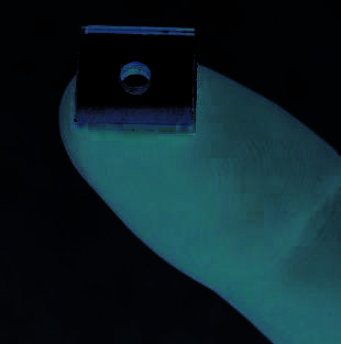
Fig. 37. Desktop real-time PCR device co-working with silicon-glass reusable chips: a) view
of the instrument, b) 1 cm x 1 cm chip on author’s finer
The second interesting application of the miniature semiconductor laser and CCD-based
detection unit is a portable cocaine detector developed under European project
LABONFOIL (Walczak at al. 2009). The cocaine test is forecasted to be used as prevention
test for professional drivers of heavy trucks or buses. The device consist of a disposable
wearable cartridge with implemented biological part for cocaine/metabolite detection in a
human sweat sample and a hand-held optical reader connected to a computer. The
disposable cartridge contains lab-on-a-paper for sweat sample collection and
immunochromatography-based cocaine or its metabolite separation and detection. The
hand-held reader utilizes semiconductor red laser diode in the excitation channel and 670
nm interference filter co-working with the minicamera in the fluorescence readout channel.
The reader is supplied by USB port of a portable computer (Fig. 38). Preliminary tests of the
instrumentation confirmed high sensitivity of the optical reader. Lowest detection limit of
t