)Ve 8
pos
(m
de
o
4
at
rgyen
0
E
0
100
200
300
400
Target bias volt age (V)
Fig. 18. Evolution of the energy deposited by condensing Pt atoms as a function of the target
bias voltage
It is seen from Figure 18 that the energy deposited per atom does not depend on the target
bias voltage (in the investigated range). This is in agreement with what is reported in
literature [31] and results of our calculations [28]. Indeed, in our ranges of experimental
parameters, the kinetic energy of sputtered atoms depends on the gas pressure rather than
on the target voltage. The value that can be deduced from the graph is 10.8 eV, which has to
be compared to the energy which a Pt atom may release at the substrate surface. Pt atoms
carry a kinetic energy estimated to 4.9 eV in the present conditions (0.5 Pa, 10 cm from the
target) and transfer their condensation energy, i.e. 5.3 eV, which gives 10.2 eV. The good
agreement between calculated and measured values indicates that Pt atoms transfer their
whole energy to the surface.
One can wonder if the same energy brought by different species would affects the thin film
growth in the same manner. In order to study the role of the energetic vector, deposition of
Pt thin films was performed at different locations in the reactor presented in Figure 14. The
energetic contributions of both the Ar plasma and the condensing atoms vary. Both
contributions are displayed versus the position in the reactor in figure 19. As already
reported, in our conditions, the contribution of the plasma is widely higher than the
SPD one.
Thin films were deposited at 3 cm and 18 cm from the target. They were analyzed by
scanning electron microscopy (SEM) and Rutherford backscattering spectroscopy (RBS).
Results are given in figure 20 and Table 4.


106
Microsensors
)-2 400
.cm
350
Wm 300
25
ty (
250
ity
20
nsi
ns
200
e
2)
de
15
d
150
lux
/cm
lux
f
W 10
100
rgy
(m
gy f
50
5
er
Ene
0
En
0
0
5
10
15
0
5
10
15
20
Target/substrate distance (cm)
Target/substrate distance (cm)
a) (b)
Fig. 19. Evolution of a) plasma and b) SPD energetic contributions versus the distance
between the target and the substrate
20nm
50nm
(a)
(b)
50nm
100nm
(c)
(d)
Fig. 20. SEM images of Pt thin films synthesized at 0.5Pa, 400W and -200V target bias
voltage ; (a) and (b) target/substrate distance of 18 cm, 30 min deposition time ; (c) and (d)
target/substrate distance of 3 cm, 11 min 30 s deposition time.
Thickness
Thickness
Pt atom number
Deposition rate
Echantillon
calculated from measured on SEM
(RBS) (at/cm2)
(at/cm2s)
RBS (nm)
images (nm)
30min, 18cm
1.11017
17 31
6.11013
11min30s, 3cm
8.51017
128 130
1.21015
Table 4. Results from SEM images and RBS. The thickness is determined from RBS results by
assuming that the film density is the same as the bulk one. The comparison with the value
measured on SEM images gives some insight into the film density.
A Heat Flux Microsensor for Direct Measurements in Plasma Surface Interactions
107
It is seen from the results above that the Pt film synthesized close to the target
(target/substrate distance of 3 cm) is denser and more compact that the one deposited 18 cm
away. The energetic deposition conditions deduced from figure 18 are given below:
-
distance of 3cm
plasma= 160 mW/cm2 and dep = 24 mW/cm2
global = 184 mW/cm2
-
distance of 18cm
plasma= 300 mW/cm2 and dep = 8 mW/cm2
global = 308 mW/cm2
It is interesting to note that the global transferred energy is higher far from the target
because the Ar plasma contains the most energy at this location. However, the obtained
films exhibit low density, which is usually attributed to a growth process that takes place
when low energy is available at the surface [20]. Indeed, our results show that the energetic
contribution that drives the film characteristics is the energy deposited by the condensing
atoms, which is higher at 3 cm. The fact that a minor contribution might play the major role
had never been reported until now. This indicates that, as usually done, discussing film
properties by only taking account the the most abundant species or the one that carries the
more energy is not accurate.
7. Conclusions
We have shown that the plasma energy flux probe we have developed from a commercial
sensor is a relevant and innovative plasma diagnostic. It is able to give direct measurement
of the energy influx from the plasma to a surface. The sensor has to be calibrated following a
rigorous procedure so that it can be used in low pressure plasmas. We have compared the
values given by this sensor to the ones obtained using an other technique developed by
colleagues from Kiel [17] and we found a very good agreement between both probes. The
main advantages of this sensor rely on the fact that it has a very good time response (17 µs
[5]) and that it does not need further data treatment, but gives directly the measured values
in real time. This very good time resolution is obtained because of the very thin films, which
form the thermopile. The sensitivity of this new sensor was tested in different experiments
such as Argon plasma, silicon etching plasma and sputtering deposition plasmas. In all
cases, it gave valuable information and measured values were in good agreement with
estimations from indirect methods.
This sensor in its commercially available version is well adapted for measurements onto
small samples (typically 1 cm²). However, we have shown that it is of particular importance
to avoid all kinds of heat flux leaks. If a small thermal bridge is obtained by putting an
additional mechanical piece on the sample (for example to fix it), then it will impact the
measurement. This is why we decided to just stick the different samples to the sensor
directly with a thermal paste.
We are now trying to improve the sensor to make it able to measure the energy flux in other
conditions. For example, this sensor would be even more of interest for the plasma
community if it could be biased. In this case, we would be able to enhance the ion
bombardment and evaluate its impact on the energy influx.
This new method in determining the energy influx has opened new research perspectives in
the plasma community, especially for materials processing.
108
Microsensors
8. References
[1] S. Aida and S. Rahmane, Thin Solid Films 288, 83 (1996)
[2] A. Durandet, O. Joubert, J. Pelletier, and M. Pichot, J. Appl. Phys. 67, 3862 (1990)
[3] H. Kersten et Al, Vacuum 63, 385 (2001)
[4] A.L. Thomann et al., Rev. Scient. Instr., 77, 033501 (2006)
[5] http://www.vatell.com
[6] F. P. Incropera, D. P. DeWitt, Introduction to Heat Transfer, 4th ed, Wiley, 93-95,(2002).X.
[7] Zhang , P.Z. Cong and M. Fujii, A Study on Thermal contact resistance at the interface of
two solids, International Journal of Thermophysics, 27 (3), 880-895, (2006)
[8] M. J. Persky, Review of black surfaces for space-borne infrared systems, Review of
Scientific Instruments, 70 (5), 2193-2217 (1999).
[9] F. M. Devienne, Advances in Heat Transfer, Low Density Heat Transfer, 272-352(1965).
[10] J. A. Thornton J A 1978 Thin Solid Film 54 23
[11] D. J. Ball 1972 J. Appl. Phys. 43 3047
[12] R. Gardon 1953 The Rev. of Sci. Instrum. 24 366
[13] C. Paturaud, G. Farges, M. C. Sainte Catherine and J. Machet 1998 Surf. Coat. Technol.
98 1257
[14] R. Piejak R, V. Godyak, B. Alexandrovich and N. Tishchenko 1998 Plasma Sources Sci.
Technol. 7 590
[15] Drüsedau T P, Bock T, John T-M, Klabunde F and Eckstein W 1999 J. Vac. Sci. Technol.
A 17(5) 2896
[16] Drüsedau T P, Löhmann M, Klabunde F and John T-M 2000 Surf. Coat. Technol. 133–
134 126
[17] Kersten H, Wiese R, Hannemann M, Kapitov A, Scholze F, Neumann H and Hippler R
2005 Surf. Coat. Technol. 200 809
[18] Ellmer K and Mientus R 1999 Surf. Coat. Technol. 116–119 1102
[19] Thornton J A and Lamb J L 1984 Thin Solid Films 119 87
[20] Kersten H, Rohde D, Steffen H, Hippler R, Swinkels G H P M and KroesenGMW2001
Appl. Phys. A 72 531
[21] Wolter M, Stahl M and Kersten H 2009 Vacuum 83 768
[22] Cormier P-A et al 2010 J. Phys. D : Appl.Phys. 43 465201
[23] Lundin D, Stahl M, Kersten H and Helmersson U 2009 J. Phys. D: Appl. Phys. 42 185202
[24] M. A. Lieberman and A. J. Lichtenberg, « Principles of Plasma Discharges and
Materials » Processing Wiley, New York (1994)
[25] Ch.Cardinaud, M.C.Peignon, G.Turban, “Si and W etching mechanistic study based on
in-situ surface temperature measurements” , International Symposium on Plasma
Chemistry 11, Loughborough, UK, August 22-27, 1993, Edited by J. Harry
[26] R. Dussart, A. L. Thomann, L. E. Pichon, L. Bedra, N. Semmar, P. Lefaucheux,
J. Mathias, and Y. Tessier, “Direct measurements of the energy flux due to chemical
reactions at the surface of a silicon sample interacting with a SF6 plasma” Applied
Physics Letters 93, 131502 (2008)
[27] Bedra L, Thomann A L, Semmar N, Dussart R and Mathias J 2010 J. Phys. D: Appl.
Phys. 43 065202
[28] Brault P et al 2000 Recent Res. Dev. Vac. Sci. Technol. 2 35
[29] Wendt R, Ellmer K and Wiesemann 1997 J. Appl. Phys. 82 2115
[30] Yamamura Y, Tawara H 1995 NIFS-Data Ser. 23 1
[31] J. A. Thornton, Thin Solid Films 54, 23 (1978).
5
Microsensors for Microreaction and
Lab-on-a-chip Applications
Pawel Knapkiewicz and Rafal Walczak
Wroclaw University of Technology
Poland
1. Introduction
Since the first successful applications of the microfluidical devices, measurement of
physical, chemical and biochemical parameters of performed reactions and analysis became
next challenge and millstone towards successful application of developed instrumentation
in many field of science and industry, as well as, deeper understating of micro- and nano-
world of fluidics (Ehrfeld at al., 2005). Although, methodology of these measurements was
well known from many years, the main problems that occurred were dimensional
incompatibility of available macroscopic solutions and sensing problems caused by
significant reduction of managed and analyzed volumes. Therefore, microsensors became
important part of the microfluidical device enabling real-time and on-chip measurement of
measurable parameters like pressure, temperature, conductivity, absorbance or
fluorescence.
In this chapter miniature on-chip integrated pressure sensors, discreet corrosion resistant
pressure sensor and conductometric flow-through detector will be described in details.
Nevertheless, optical microrensors like absorbance NIR and VIS detector, as well as
fluorometric detector will be shown. Technology of the sensors utilizes microengineering
techniques where silicon and glass play main role as constructional materials. Three-
dimensional formation and assembling techniques of silicon and glass allow to fabricate
miniature sensors. For each presented microsensor, the fabrication techniques will be
described in details. Great attention is also paid for development of the complete
measurement system consisting of the microsensors itself but also specialized electronics
and information environment for full data management and measurement or analyse result
presentation.
2. Miniature sensors and measurement systems for microreaction
technology
Pressure and temperature are two the most important parameters of chemical reactions.
Steering of those parameters determine chemical reaction course, as well as temperature and
pressure inform about actual chemical reaction state. Continues monitoring of temperature
and pressure is very important for exothermic, high-speed chemical reactions (Edited by
Dietrich, 2009). It can be done relatively easy for standard, macro-scale chemical plants.
Commercially available sensors are suitable to large apparatus, can be easy applied and
110
Microsensors
operate as a part of some automation systems. The microreaction technology stays in
opposite to this situation. Chemical reactions are performed in the microscale by the use of
microreactors, replacing static chemical reactions by continues-flow reactions.
Unfortunately, there is no ready-to-use sensors suitable to the microreactors. Total inner
volume of the microreactors is in the range from several µl to few ml, when external
dimensions, as well as “dead” volume of available standard sensors are at least ten times
larger, in comparison. In consequence, commercially available sensors can not work in
tandem with the microreactors.
Let’s focus our attention on extremely dangerous, highly exothermic chemical reaction, eg.
nitration of organic compounds (Ali at al., 2005; Speight, 2002), where continues monitoring
of pressure and temperature inside the microreactor is absolutely required from safety point
of view. Moreover, real-time measured data are helpful for conscious steering of chemical
reaction, towards high yield (Kralish & Kreisel, 2007).
In this paragraph miniature temperature and pressure sensors, as well as measurement
systems dedicated to the microreaction technology will be described. Several requirements
of parameters of the sensors and sensors assembling method must be considered:
-
temperature sensors operating range: -20°C ÷ +100°C,
-
dimensions of the temperature sensors should not exceed typical dimensions of
microchannels (typical dimensions are in range of tens µm up to several mm – the
average is 1 mm),
-
pressure sensors operating range: relative pressure 0 kPa ÷ 400 kPa, overpressure up to
600 kPa,
-
“dead” volume of all pressure sensors integrated to microreactor should not exceed
1/10 of total inner volume of microreactor,
-
microreactor with sensors work in harsh environment (concentrated acids, organic
compounds),
-
chemically resistance assembling required.
In the current paragraph hole process, including temperature sensors selection, pressure
sensors development, assembling and packaging problems, as well as electronics and
software realization, towards complete sensoric system for microreaction technology, will be
described in details.
2.1 Temperature sensors
Temperature sensors working in a tandem with microreactor must be characterized by small
dimensions, fast response and small measurement error. Sensor can be localised inside
microchannel (direct contact to medium) or outside microchannel (indirect contactless
measurement).
Direct sensor-to-medium contact gives most precision measurement. Thin film sensors
evaporated onto inner walls of microchannel will not survive aggressive chemicals.
Moreover, thin film technology is difficult. Discrete temperature sensors can be assembled
in the microchannel only by gluing. Both ideas do not fulfil previously listed requirements,
what in consequence eliminates this measurement idea and technical realization from the
use.
Second method is based on sensor localized outside microchannel. Main requirement is to
keep distance between sensor and medium as small as possible to allow to conduct a heat
flux with minimum losses.
Microsensors for Microreaction and Lab-on-a-chip Applications
111
Several types of commercially available sensors can be investigated. Main parameters of
commercially available sensors are collected in Table 1.
Parameter Operating range Output signal Tolerance
Housing/Dimensions
Type/model
SMD2 0805, SMD 1206, TO92,
Pt100 / Pt500 /
-200°C ÷ +860°C
Resistance,
≤ 0.3%
SOT223, ceramic or metal tube
Pt1000
(depending on type) linear PTC1
ø ≥ 1.5 mm, other
Resistance,
-55°C ÷ +150°C
SMD 0603, SMD 0805, pill-
Thermistor NTC
non-linear
1% ÷ 10%
(depending on type)
like ø ≥ 0.8 mm
NTC3
-200°C ÷ +1820°C
Voltage,
Thermocouples
±0.5°C ÷ ±4°C
metal tube ø ≥ 0.15 mm
(depending on type)
linear
Transducers with -55°C ÷ +155°C
Voltage,
0.5% ÷ 5%
all electronic standards
analogue output (depending on type) linear (usually)
digital,
Transducers with -55°C ÷ +155°C
serial data
0.5% ÷ 5%
all electronic standards
digital output (depending on type)
transfer
Table 1. Temperature sensors and their main parameters
The most common are transducers with analogue output. Output voltage signal is linear in
relation to the measured temperature and easy to measure. No additional electronic circuits
are required to process the signal. Second, most useful are transducers with digital output.
The only difference to previous one is, that digital processing by a microcontroller is
required. Unfortunately, even the smallest package of temperature transducers (SOT23
electronic standard, plastic body dimensions without electrical connections: 2.9 x 1.3 x 0.85
mm3) seams to be too large to be directly applied in microreation technology (Fig. 1a).
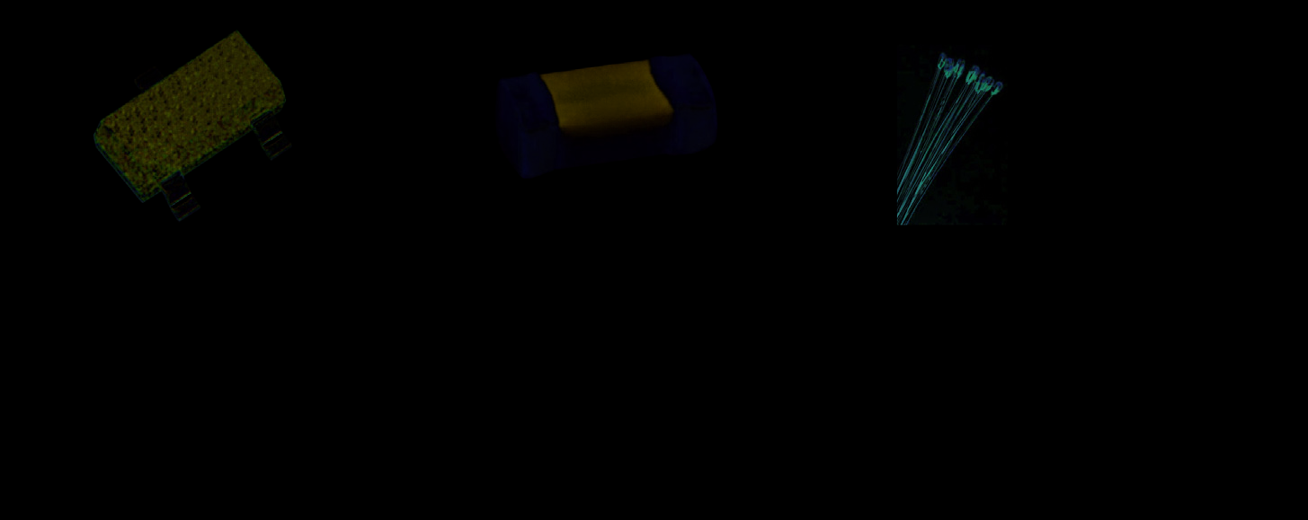
Fig. 1. Examples of miniature temperature sensors: a) temperature transducer in SOT23
package, b) PTC platinum thermoresistor (Pt-series) at 0603 SMD package, c) pill-like NTC
thermistor
1 PTC – Positive Thermal Coefficient
2 SMD – Surface Mounted Devices
3 NTC – Negative Thermal Coefficient
112
Microsensors
Different packages and dimensions of resistance PTC or NTC sensors and thermocouples
are available. Platinum temperature sensors (Pt-series) are very accurate and are used as
temperature standards. Dimensions of the ceramic or metal tube packages, as well as SMD
packages, do not fulfil harsh-environment microreaction requirements (Fig. 1b). NTC
thermistors are available in different SMD packages, including miniature pill-like packages
distinctive from others (Fig. 1c). The smallest pill-like package has 0.8 mm diameter, what is
suitable to mentioned earlier requirements. Thermocouples are usually packaged in the
metal tubes. Special constructions are available in tubes of 0.15 mm in diameter. It is the
smallest dimension (diameter) of all sensors discussed before. In spite of that,
thermocouples need to co-work with sophisticated electronic circuits.
The analysis of commercially available temperature sensors appoints that the miniature
pill-like NTC thermistors as the best solution. Small glass package, thin and flexible
electrical wires entail small thermal capacity and fast response.
The location of miniature pill-like NTC thermistors onto microreactors made of glass, silicon
and glass as cover, ceramics, polymers, was proposed. Sensor should be located inside
“blind” hole of 1.0 mm in maximum diameter, fabricated directly above microchannel. The
optimal distance of 200 µm between medium and temperature sensor has been found
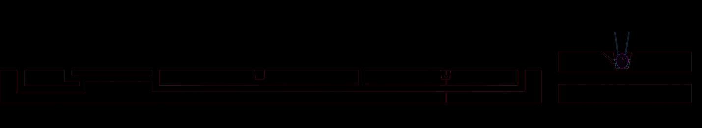
experimentally to be optimal. The schematic cross-section of a microreactor with NTC
thermistor and the sensor integration to glass-silicon-glass microreactor is schematically
presented on Fig. 2.
Fig. 2. Indirect temperature measurement: cross-section of a microreactor (left) and NTC
thermistor location (right)
Thermal behaviours of the glass-silicon-glass microreactor equipped with miniature pill-like
NTC thermistors will be widely discussed later in paragraph 2.3.
2.2 Pressure sensors
As it was mentioned before, required operation range of pressure sensors is from 0 kPa to
400 kPa of relative pressure. 400 kPa is a maximum operating pressure of microreactors
made of glass, silicon-glass, c