typically observed nanotubular layers) can simply be obtained by controlling the water
content in the electrolyte during the anodization process. It is proposed that the morphology
transition from pores to tubes is based on the rate of preferential etching at the hexagonal
cell triple points in the oxide.
Zhang prepared the highly ordered TiO2 thin films by anodic oxidation followed by
calcination at various temperatures (300, 400, 500 and 600 °C) (Zhang, 2008). The author
investigated the humidity sensing behaviours of prepared samples. The samples calcined at
600 °C showed high sensitivity with nearly two orders change in the resistance and short
response and recovery time (< 190 s) during the relative humidity variation from 11 to 95%.
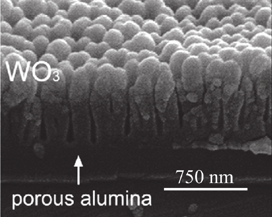
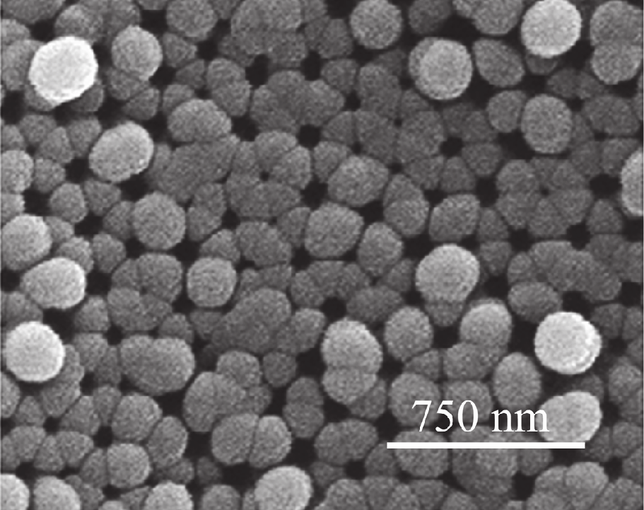
Another method is the deposition of WO3 thin films on highly ordered nanoporous alumina
template. Nanoporous anodic oxide layers were formed by anodizing aluminum films in
malonic acid electrolyte. Tungsten trioxide sensing films were deposited on the top of
nanoporous alumina layers by rf magnetron sputtering of a metallic target (Fig. 7). The
tungsten oxide gas sensing structures supported by nanoporous alumina templates showed
high responsiveness to toxic gases, especially to NO2 (Gorokh, 2006; Khatko, 2009, 2006;
Vallejos, 2008).
Chemical Microsensors with Ordered Nanostructures
155
Fig. 7. SEM images of cross-fracture (left) and the surface (right) of alumina films with
sputtered WO3
4. Conclusion
Described non-litographic techniques are based on template-assisted method. The template preparation of thin film with highly ordered pores is a suitable way for nanostructured
material synthesis since they are cheap, fast and easy reproducible. Due to the special
properties arising from their behavior, these highly ordered nanostructures can find various
applications in environmental analysis as well as medicine and pharmacy.
In the case of environmental analysis application, the nanostructures are used to modify
either the sensing elements from the semiconducting materials of vapor and gas sensors or
the electrodes of electrochemical sensors.
Concerning the pharmacy and medicine, quantum dots (QDs) in planar form (so-called lab-
on-chip) deposited on various solid surfaces seems to be a new approach of template-based
method application. The sensor array created from separately deposited QDs, also called
“fluorescence array detector”, can be used for in-vitro large-field imaging. This allows the
easy detection of many different biomolecules at the same time, since each QD can emit the
light at different wavelength. Electrochemical biosensors with functionalized electrodes for
rapid detection and mass screening are very promising in near future in cases of pandemic
and epidemic. Cultivation of cells on gold nanodots has also high impact in biochemistry
research for medicine.
5. Acknowledgment
This work has been supported by Grant Agency of the Academy of Sciencies of the Czech
Republic under the contract GAAV KAN208130801 (NANOSEMED) and by Grant Agency
of the Czech Republic under the contract GACR 102/08/1546 (NANIMEL).
6. References
Alivov, Y. et al. (2009). Titanium nanotubes grown by titanium anodization. Journal of Applied
Physics, Vol. 106, No. 3, pp. 5, ISSN 0021-8979
Alonso-Gonzalez, P. et al. (2006). Ordered InAs QDs using prepatterned substrates by
monolithically integrated porous alumina. Journal of Crystal Growth, Vol. 294, No. 2,
pp. 168-173, ISSN 0022-0248
156
Microsensors
Anitha, V. C. et al. (2010). Electrochemical tuning of titania nanotube morphology in inhibitor
electrolytes. Electrochimica Acta, Vol. 55, No. 11, pp. 3703-3713, ISSN 0013-4686
Berger, S. et al. (2008). Formation of hexagonally ordered nanoporous anodic zirconia.
Electrochemistry Communications, Vol. 10, No. 12, pp. 1916-1919, ISSN 1388-2481
Cao, C. B. et al. (2010). Layer-by-Layer Growth Mechanism of TiO2 Nanotube Arrays. Journal
of the Electrochemical Society, Vol. 158, No. 1, pp. E8-E11, ISSN 0013-4651
Cao, G. Z. & Liu, D. W. (2008). Template-based synthesis of nanorod, nanowire, and
nanotube arrays. Advances in Colloid and Interface Science, Vol. 136, No. 1-2, pp. 45-
64, ISSN 0001-8686
Gorokh, G. et al. (2006). Anodic formation of low-aspect-ratio porous alumina films for metal-
oxide sensor application. Electrochimica Acta, Vol. 52, No. 4, pp. 1771-1780, ISSN 0013-
4686
Graham, A. H. D. et al. (2010). Nanostructured electrodes for biocompatible CMOS integrated
circuits. Sensors and Actuators B-Chemical, Vol. 147, No. 2, pp. 697-706, ISSN 0925-4005
Hahn, R. et al. (2010). Bright visible luminescence of self-organized ZrO2 nanotubes. Journal
of Solid State Electrochemistry, Vol. 14, No. 2, pp. 285-288, ISSN 1432-8488
Hassan, F. M. B. et al. (2009). Formation of Self-Ordered TiO2 Nanotubes by Electrochemical
Anodization of Titanium in 2-Propanol/NH4F. Journal of the Electrochemical Society,
Vol. 156, No. 12, pp. K227-K232, ISSN 0013-4651
Hrdý, R. & Hubálek, J. (2007). Using a Porous Alumina Film as a Mask for Formation of
Ordered Nanostructures by Deposition Technique, Acta Metallurgica Slovaca, Vol.
13, No. 2, pp. 155-158, ISSN 1335-1532
Hrdy, R. & Hubalek, J. (2005). Self ordered Pore Structure of Anodized Alumina Thin Film
on Si Substrate, Proceedings of Electronic Devices and Systems, pp. 300-304, ISBN 80-
214-2990-9, Brno, Czech Republic, September, 2005
Hu, M. Z. et al. (2009). Synthesis and characterization of anodized titanium-oxide nanotube
arrays. Journal of Materials Science, Vol. 44, No. 11, pp. 2820-2827, ISSN 0022-2461
Cha, Y. K. et al. (2004). Nonlithographic SiO2 nanodot arrays via template synthesis
approach. Japanese Journal of Applied Physics Part 1-Regular Papers Short Notes &
Review Papers, Vol. 43, No. 8A, pp. 5657-5659, ISSN 0021-4922
Chen, P. L. et al. (2005). Fabrication and field emission characteristics of highly ordered
titanium oxide nanodot arrays. Electrochemical and Solid State Letters, Vol. 8, No. 10,
pp. H83-H86, ISSN 1099-0062
Chen, P. L. et al. (2004). Preparation and phase transformation of highly ordered TiO2
nanodot arrays on sapphire substrates. Applied Physics Letters, Vol. 84, No. 19, pp.
3888-3890, ISSN 0003-6951
Chen, P. L. et al. (2003). Self-organized titanium oxide nanodot arrays by electrochemical
anodization. Applied Physics Letters, Vol. 82, No. 17, pp. 2796-2798, ISSN 0003-6951
Cho, S. J. et al. (2008). Titanium oxide nanotubes anodized in aqueous and non-aqueous
electrolytes. Journal of Ceramic Processing Research, Vol. 9, No. 5, pp. 449-451, 1229-9162
Chu, S. Z. et al. (2005). Self-organized nanoporous anodic titania films and ordered titania
nanodots/nanorods on glass. Advanced Functional Materials, Vol. 15, No. 8, pp. 1343-
1349, ISSN 1616-301X
Chu, S. Z. et al. (2005). A new electrochemical lithography - Fabrication of self-organized
titania nanostructures on glass by combined anodization. Journal of the
Electrochemical Society, Vol. 152, No. 3, pp. B116-B124, ISSN 0013-4651
Joo, S. et al. (2010). Hydrogen Gas Sensor Using Pt- and Pd-Added Anodic TiO2 Nanotube
Films. Journal of the Electrochemical Society, Vol. 157, No. 6, pp. J221-J226, ISSN
0013-4651
Chemical Microsensors with Ordered Nanostructures
157
Jung, J. S. et al. (2008). Electrodeposited Nickel Nanodots Array on the Silicon Wafer. Bulletin
of the Korean Chemical Society, Vol. 29, No. 11, pp. 2169-2171, ISSN 0253-2964
Jung, M. et al. (2006). Fabrication of the uniform CdTe quantum dot array on GaAs substrate
utilizing nanoporous alumina masks. Current Applied Physics, Vol. 6, No. 6, pp.
1016-1019, 1567-1739
Kemell, M. et al. (2007). Atomic layer deposition of nanostructured TiO2 photocatalysts via
template approach. Chemistry of Materials, Vol. 19, No. 7, pp. 1816-1820, ISSN 0897-4756
Khatko, V. et al. (2006). Tungsten trioxide sensing layers on highly ordered nanoporous
alumina template. Sensors and Actuators B-Chemical, Vol. 118, No. 1-2, pp. 255-262,
0925-4005
Khatko, V. et al. (2009). Micro-machined WO3-based sensors with improved characteristics.
Sensors and Actuators B-Chemical, Vol. 140, No. 2, pp. 356-362, ISSN 0925-4005
Klosová, K. & Hubálek, J. (2008). Advanced electrodes with nanostructured surfaces for
electrochemical microsensors, Physica Status Solidi, Vol. 205, No. 6, pp. 1435-1438,
ISSN 0031-8965
Klosova, K. et al. (2006). New Microelectrodes for Electrochemical Application with
Nanomachined Surface, Proceedings of the International Conference NANO´06, pp.
210-214, ISBN 80-214-3331-0, Brno, Czech Republic, November, 2006
Klosova, K. et al. (2006). New Approach to Electrochemical Sensor Electrodes Construction,
Proceedings of Junior Scientist Conference, pp. 139-140, ISBN 3-902463-05-8, Vienna,
Austria, April, 2006
Kokonou, M. et al. (2007). Few nanometer thick anodic porous alumina films on silicon with
high density of vertical pores. Thin Solid Films, Vol. 515, No. 7-8, pp. 3602-3606,
ISSN 0040-6090
Kouklin, N. et al. Capacitance-voltage spectroscopy of self assembled ordered arrays of
quantum dots. New York: Ieee, 2000.
Li, A. P. et al. (1998). Hexagonal pore arrays with a 50-420 nm interpore distance formed by
self-organization in anodic alumina. Journal of Applied Physics, Vol. 84, No. 11, pp.
6023-6026, ISSN 0021-8979
Li, C. P. et al. (2006). Fabrication and structural characterization of highly ordered sub-100-
nm planar magnetic nanodot arrays over 1 cm(2) coverage area. Journal of Applied
Physics, Vol. 100, No. 7, pp. 7, ISSN 0021-8979
Li, L. L. et al. (2010). Morphologic Characterization of Anodic Titania Nanotube Arrays for
Dye-Sensitized Solar Cells. Journal of the Chinese Chemical Society, Vol. 58, No. 5B,
pp. 1147-1150, ISSN 0009-4536
Liang, J. Y. et al. (2002). Two-dimensional lateral superlattices of nanostructures:
Nonlithographic formation by anodic membrane template. Journal of Applied
Physics, Vol. 91, No. 4, pp. 2544-2546, ISSN 0021-8979
Lim, J. H. et al. (2009). Electrochemical determination of whole blood clotting time by using
nanodot arrays. Electrochemistry Communications, Vol. 11, No. 11, pp. 2141-2144,
ISSN 1388-2481
Liu, Y. B. et al. (2009). Comparison of photoelectrochemical properties of TiO2-nanotube-
array photoanode prepared by anodization in different electrolyte. Environmental
Chemistry Letters, Vol. 7, No. 4, pp. 363-368, ISSN 1610-3653
Mao, R. et al. (2009). In situ preparation of an ultra-thin nanomask on a silicon wafer.
Nanotechnology, Vol. 20, No. 2, pp. 6, ISSN 0957-4484
Masuda, H. & Fukuda, K. (1995). Ordered metal nanohole arrays made by a 2-step
replication of honeycomb structures of anodic alumina. Science, Vol. 268, No. 5216,
pp. 1466-1468, ISSN 0036-8075
158
Microsensors
Masuda, H. et al. (1998). Self-ordering of cell configuration of anodic porous alumina with
large-size pores in phosphoric acid solution. Japanese Journal of Applied Physics Part
2-Letters, Vol. 37, No. 11A, pp. L1340-L1342,
Matefi-Tempfli, S. et al. (2009). Nanowires and nanostructures fabrication using template
methods: a step forward to real devices combining electrochemical synthesis with
lithographic techniques. Journal of Materials Science-Materials in Electronics, Vol. 20,
No., pp. 249-254, ISSN 0957-4522
Montero-Moreno, J. M. et al. (2009). Production of alumina templates suitable for
electrodeposition of nanostructures using stepped techniques. Electrochimica Acta,
Vol. 54, No. 9, pp. 2529-2535, ISSN 0013-4686
Mozalev, A. et al. (2009). Growth of multioxide planar film with the nanoscale inner
structure via anodizing Al/Ta layers on Si. Electrochimica Acta, Vol. 54, No. 3, pp.
935-945, ISSN 0013-4686
Mun, K. et al. (2010). A Stable, Label-free Optical Interferometric Biosensor Based on TiO2
Nanotube Arrays. Acs Nano, Vol. 4, No. 4, pp. 2070-2076, ISSN 1936-0851
Oide, A. et al. (2006). Fabrication of ordered nanostructure on silicon substrate using
localized anodization and chemical etching. Electrochemistry, Vol. 74, No. 5, pp. 379-
384, ISSN 1344-3542
Possin, G. E. (1970). A method for forming very small diameter wires. Review of Scientific
Instruments, Vol. 41, No. 5, pp. 772-&, ISSN 0034-6748
Sennik, E. et al. (2010). Synthesis of highly-ordered TiO2 nanotubes for a hydrogen sensor.
International Journal of Hydrogen Energy, Vol. 35, No. 9, pp. 4420-4427, ISSN 0360-3199
Shingubara, S. (2003). Fabrication of nanomaterials using porous alumina templates . Journal
of Nanoparticle Research, Vol. 5, No. 1-2, pp. 17-30, ISSN 1388-0764
Song, Y. Y. & Schmuki, P. (2010). Modulated TiO2 nanotube stacks and their use in
interference sensors. Electrochemistry Communications, Vol. 12, No. 4, pp. 579-582,
ISSN 1388-2481
Tan, L. K. et al. (2010). Transparent, Well-Aligned TiO2 Nanotube Arrays with Controllable
Dimensions on Glass Substrates for Photocatalytic Applications. Acs Applied
Materials & Interfaces, Vol. 2, No. 2, pp. 498-503, ISSN 1944-8244
Vallejos, S. et al. (2008). Micro-machined WO3-based sensors selective to oxidizing gases.
Sensors and Actuators B-Chemical, Vol. 132, No. 1, pp. 209-215, ISSN 0925-4005
Vorozhtsova, M. et al. (2010). Ta2O5 Nanocrystals Created by Anodization, Proceedings of X.
Workshop of Physical Chemists and Electrochemists, pp. 259 - 261, ISBN 978-80-7375-
396-2, Brno, Czech Republic, June, 2010
Wang, A. W. & White, R. M. (1995). Thin-film anodized aluminum on an acoustic sensor. In:
Ieee Ultrasonics Symposium Proceedings, Vols 1 and 2, Levy, Schneider, McAvoy, pp.
437-440, IEEE, ISBN 1051-0117, New York
Wang, C. C. et al. (2007). Organic nanowire-templated fabrication of alumina nanotubes by
atomic layer deposition. Nano Letters, Vol. 7, No. 6, pp. 1566-1569, ISSN 1530-6984
Wang, H. W. et al. (2006). Standing [111] gold nanotube to nanorod arrays via template
growth. Nanotechnology, Vol. 17, No. 10, pp. 2689-2694, ISSN 0957-4484
Wang, J. G. et al. (2004). Microstructure and interdiffusion of template-synthesized Au/Sn/Au
junction nanowires. Nano Letters, Vol. 4, No. 7, pp. 1313-1318, ISSN 1530-6984
Wang, Q. et al. (2010). Resistive and capacitive response of nitrogen-doped TiO2 nanotubes
film humidity sensor. Nanotechnology, Vol. 22, No. 2, pp. 11, ISSN 0957-4484
Wang, Y. et al. (2005). Synthesis and electrochemical properties of vanadium pentoxide
nanotube arrays. Journal of Physical Chemistry B, Vol. 109, No. 8, pp. 3085-3088, ISSN
1520-6106
Part 3
Optical Microsensors
7
Surface-Enhanced Raman Scattering Sensors
based on Hybrid Nanoparticles
Rafael Contreras-Cáceres, Benjamín Sierra-Martín and
Antonio Fernández-Barbero
Applied Physics Department, University of Almería
Spain
1. Introduction
Surface-enhanced Raman scattering (SERS) is a powerful vibrational spectroscopic
technique that allows ultra-sensitive chemical or biochemical analysis (Kneipp, Kneipp et
al. 1999). It works by increasing the Raman signal of analyte molecules located nearby the
surface of metallic nanostructures that can undergo localized surface plasmon resonance.
Among these nanostructures, gold and silver nanoparticles are the dominant substrates, for
both experimental and theoretical perspectives (Kneipp, Wang et al. 1997; Nie and Emery
1997), since they can support plasmon resonance properties able to increase the Raman
signal up to 14 or 15 orders of magnitude, high enough to detect single molecules (Nie and
Emery 1997; Qian and Nie 2008). Since the first report concerning the enhanced Raman
signal of pyridine molecules adsorbed on a roughened silver electrode (Fleischm, Hendra et
al. 1974), considerable efforts have been made in understanding the SERS mechanisms
(Schatz 1984; Campion and Kambhampati 1998). Nowadays, analytical applications have
centred the attention, and research is devoted to optimize the specific conditions for
detecting each particular analyte (Porter, Lipert et al. 2008). Interestingly, the enhancement
factor is found to depend on the different affinity of the functional groups in the analyte
toward gold or silver surfaces because it is the affinity which determines the analyte
retention (Pearson 1963; Pearson 1966). To improve the surface-analyte interaction, various
approaches have been developed, including the functionalization of nanoparticle surface
(Guerrini, Garcia-Ramos et al. 2006; Guerrini, Garcia-Ramos et al. 2008); however, a problem
inherent to this alternative is that usually the assembled molecules provide strong SERS
signals that overlap and screen those corresponding to the analyte. Another alternative
relies on controlling the surface charge of the nanoparticles to promote the electrostatic
attraction of the analyte onto the particle surface (Alvarez-Puebla, Arceo et al. 2005; Aroca,
Alvarez-Puebla et al. 2005). This approach has been reported to consistently enhances the
signal for acids and amines, but it hardly helps in the case of alcohols, ethers, and other
oxygen containing groups, as well as for non-functionalized molecules. Thereby, there is a
clear need for development of new nanocomposites, based on noble-metals, containing a
sensitive material that enables the physical trapping of a wide variety of analyte molecules.
Herein we present the synthesis and applications of novel core-shell nanocomposites
comprising Au and Au-Ag bimetallic cores, with spherical or rod-shaped morphology,
162
Microsensors
coated with thermally responsive poly-(N-isopropylacrylamide) (pNIPAM) microgel
(Contreras-Caceres, Sanchez-Iglesias et al. 2008). In these systems, whereas the metallic core
provides the necessary enhancing properties, the pNIPAM shell, that can swell or collapse
as a function of temperature, is used to trap the analyte molecules and get them sufficiently
close to the core. These materials present unique optical properties as a consequence of the
thermally responsive surface plasmon resonance, which can be ultimately exploited for
SERS analysis. Although similar systems have been proposed for applications in catalysis
(Lu, Mei et al. 2006), temperature or pH sensing (Kim and Lee 2004), or light-responsive
materials (Gorelikov, Field et al. 2004), we report here that the hybrid nanoparticles can
function as general sensors for detecting different types of analytes. Apart from the SERS
enhancement, these nanocomposites can also be used to modulate the fluorescence intensity
of adsorbed chromophores as a function of temperature. It is important to note, that the
pNIPAM shell not only enhances the colloidal stability of the system in aqueous solutions,
but additionally prevents electromagnetic coupling between metal particles, thus providing
highly reproducible SERS signal and intensity, which is crucial for quantitative applications.
Through a rational choice of model analytes, we report the applications of these
thermoresponsive hybrid materials for Surface Enhanced Raman Scattering and
Fluorescence (SERS and SEF, respectively). The nanocomposites are first tested using 1-
naphthalenethiol (1NAT) as a model analyte with large affinity for gold, and consecutively
against a common dye, Nile Blue A (NBA), whose affinity for gold is lower than of 1NAT. In
addition, we present the SERS analysis of 1-napthol, a substance that had remained elusive
for SERS since it does not easily adsorb onto conventional silver or gold surfaces and whose
detection is decisive because is considered a relevant biomarker (Hansen, Omland et al.
1994; Sun, Shen et al. 2008) and also causes genotoxicity under chronic exposure to humans
(Kozumbo, Agarwal et al. 1992; Grancharov, Engelberg et al. 2001). To conclude the report,
the SERS efficiency of the different hybrid nanocomposites is compared for a couple of
analytes. The wide range of systems investigated, lead us to establish the effect of
parameters, such as particle morphology or core composition, on the detection capabilities.
Interestingly, sensors based on Au-Ag core coated by the pNIPAM shell are found to
provide much higher SERS intensities than their Au-pNIPAM counterparts, not only in the
case of spheres but particularly for nanorods.
2. Plasmon resonance and surface-enhanced Raman scattering
Plasmons are quantized collective oscillations of the free electron gas density that occurs
between any two materials whose dielectric function changes sign across the interface, for
instance metal-dielectric interfaces (Barnes, Dereux et al. 2003). Surface plasmons are those
confined to surfaces; they can strongly couple with photons resulting in surface polaritons,
which are considered quasi-particles that propagate along the metal surface until its energy
decays via absorption into the metal or radiation into the free-space (Zayats, Smolyaninov et
al. 2005). Light or electric fields can excite those plasmons, then resulting in surface and
localized surface plasmon resonance (SPR and LSPR) in the case of planar and nanometric-
sized metallic structures, respectively (Mulvaney 1996). Plasmon oscillation is resonant with
the light at a particular frequency. The electric field intensity, the scattering and the
adsorption cross-sections are then enhanced. Materials exhibiting surface plasmon
properties are used to maximize surface sensitive spectroscopic techniques, such as Raman
scattering or fluorescence (Hutter and Fendler 2004). The resonance frequency strongly
Surface-Enhanced Raman Scattering Sensors based on Hybrid Nanoparticles
163
depends on the size and shape of the metal nanoparticles, as well as, on the metal complex
dielectric function and surrounding medium. Noble metals such as copper, silver, and gold
exhibit strong visible-light plasmon resonance, whereas other transition metals show only a
broad and poorly resolved absorption band in the ultraviolet region (Link and El-Sayed
1999). To understand the optical properties of these metals, it is not only necessary to
account for the effect of free-electrons, responsible for plasmon resonance, but also for the
interband transitions (Wang, Tam et al. 2005). For instance, copper nanoparticles have
strong interband transitions which overlap with the plasmon resonance energies, then
leading to a damping effect that minimizes its optical response. Contrarily, in case of gold
and silver nanoparticles, both effects are well separated in the spectrum. Therefore, electrons
of the conduction band can move freely, showing higher polarizability. This fact, in turn
shifts the plasmon resonance to lower frequencies with sharp bandwidth. Since copper is
also easily oxidized, gold and silver nanoparticles are more attractive for optics-based
applications, specifically silver since it has by