2 1/2
A ( A n / 2) 2( A r )
( A n / 2)
B
n
(n) =
.
2
2 1/2
2( A r )
2
n
A n
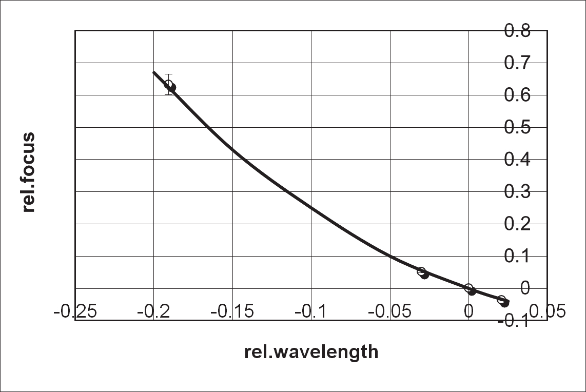
where A and B are the front and back sections or the design distances from FZP to a source and the positions, respectively, 0 is the design wavelength which in the general case
differs from the wavelength diffracting on FZP, n – number of Fresnel zone. If B is
averaged between its extreme values:
B = 0.5(B (1) + B (N)),
(1)
then expression (1) coincides, within the accuracy of calculations and measurements, with
calculations by the Kirchhoff scalar theory as /0 varies within 20% and with
experimental values for all j. These results are plotted in fig. 1.
A similar dependence for a zone plate designed for focusing a wave with planar wavefront
is:
B(p)=r2p/2N - N/2p.
Here p is the number of phase quantization levels and N is the total number of Fresnel
zones.
From the above is it followed that the FZP may be considered in the first approximation as a
circular grating characterized be a constant L=F*λ, where F is the focal length of FZP. Thus
the focal length of FZP is inversely proportional to the wavelength and is determinate by
F=L/λ. The FZP resolves the incident radiation into monochromatic components. Since each
component has its own focal point, it will be projected onto one element of the sensing array
along optical axis. This means that the N-element linear array can detect N different
wavelength components simultaneously.
It could be noted that a problem of synthesizing an amplitude-phase profile even of the
simplest diffraction element such as FZP has no unique solution [1]. Usually, radii of Fresnel
zones are determined from the condition of multiplicity to a half-wavelength of the
difference of eikonais of a diffracted direct wave and a reference wave. This solution,
however, is merely a particular case of a more general one. The essence of constructing such
a general solution is that the notion of a reference radius R0 on the aperture of a focusing element is introduced [1].
220
Microsensors
Fig. 1. The position of the focusing area as a function of wavelength of the incident radiation
3. Multiorder diffractive optics properties
Although it is often useful to think of a diffractive lens as a modulo 2π lens at the design
wavelength, the spectral properties or wavelength dependence of a diffractive lens are
drastically different from those of a refractive lens. The dispersion of a diffractive lens is
roughly 7 times larger (in optical waveband) than the strongest flint glass currently
available and is opposite in sign. The quantization of the phase function of a diffractive
element results in new properties of the element. One of these manifestations of discreteness
of the phase function of the elements that we discuss is the possibility of selecting harmonics
of coherent radiation. Analytical expressions for a four-level diffractive element were
obtained in [1] for the gain of the axisymmetric element G at the main focal point
corresponding to the reference wavelength:
2
N
G(N) =
0
0
(
A n)cos(2 M
( MGi (
v n) 1)) cos(2 M
( Gi (
v n))
+
n1
2
N
+
0
0
(
A n)sin(2 M
( MGi (
v n) 1)) sin(2 M
( Gi (
v n))
n1
4 MF
4 MF
A(n) =
2 n 1 /
M(2 n 1)
0
0
Diffractive Optics Microsensors
221
where N is the number of Fresnel zones within the aperture of the element; 0 and are the
reference and the actual radiation wavelength; F is the focal length and Giv(n) is the function
equal to the maximum integral value of its argument. So diffractive lens offers the potential for
several wavelength components of the incident spectrum to come to a common focus.
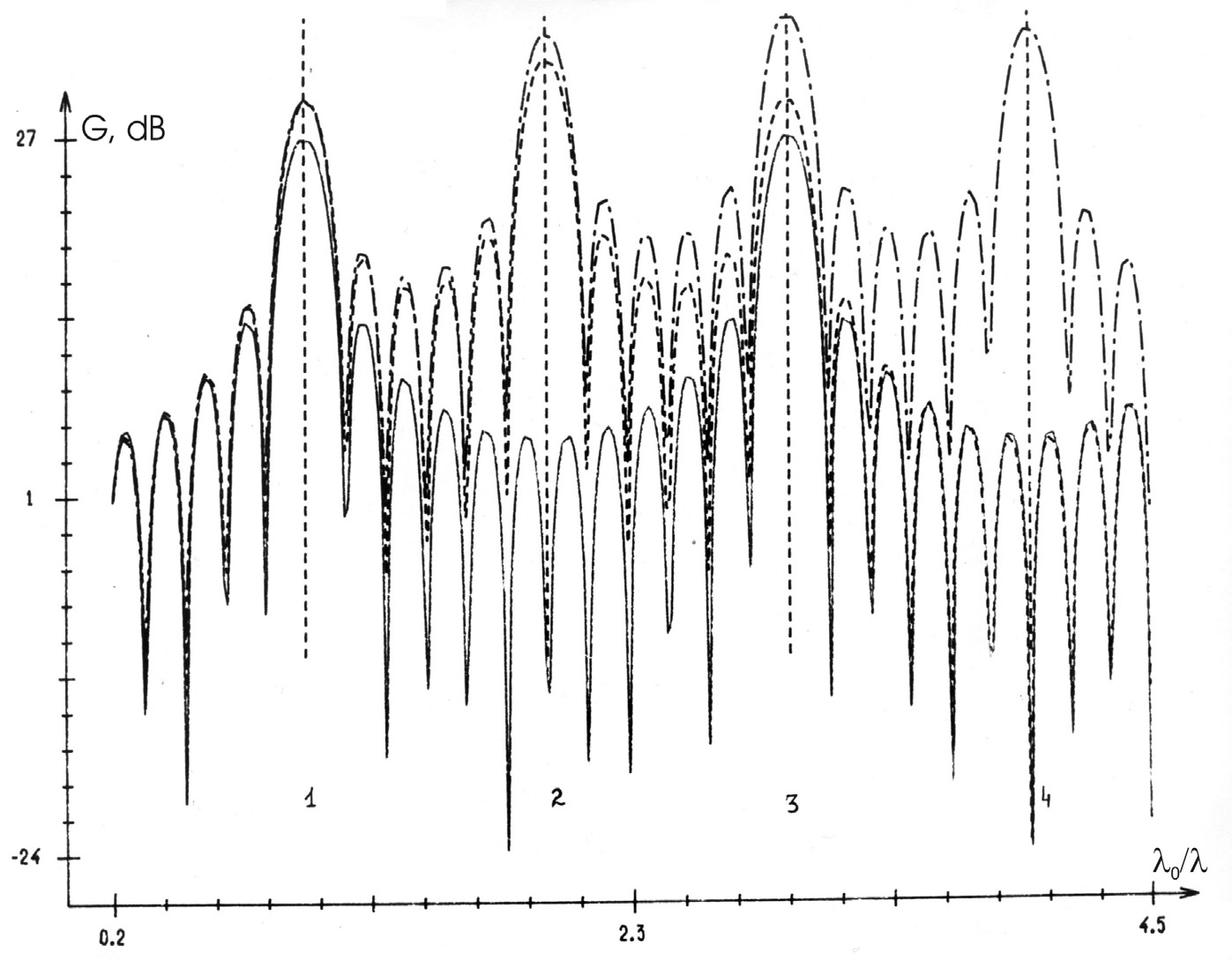
An analysis of this relation shows that the maximum gain (for constant signal-to-noise ratio)
is achieved for the harmonic with the number 0/ = M/2, while there is no focusing of
radiation at the wavelength satisfying 0/ = M, that is, this radiation is selected (fig. 2-3).
Fig. 2. Gain of a diffractive optical element for three numbers of phase quantization levels
[20]:
__________ two levels,
_ _ _ _ four levels,
_._._._._ six levels
It is important to note a well-known property of operation when higher diffracted orders are
used. The wavelength bandwidth of the diffraction efficiency around a given diffracted
order narrows with increasing values of n.
Spectrally selective properties of diffractive elements with a discrete phase function make it
possible to use them for mixing a discrete set of wavelengths into the same focusing zone
[1]. For instance, the following theorem is valid:
For radiation with harmonics i = 0/i, i = 1, ..., N in the interval Q = [1...2] to fall within
this interval, that is, i Q, it is necessary and sufficient for the maximum number of the
harmonic to be N = imax = entier(2/1), where entier(x) is the integral part of the real x.
222
Microsensors
The proof of this theorem is self-evident. The property of diffractive elements formulated
above is also important for practical applications. Thus it may be possible to use this
principle and design elements for the x-ray range of wavelengths, to design novel optical
elements for optical polychromatic computers, etc.
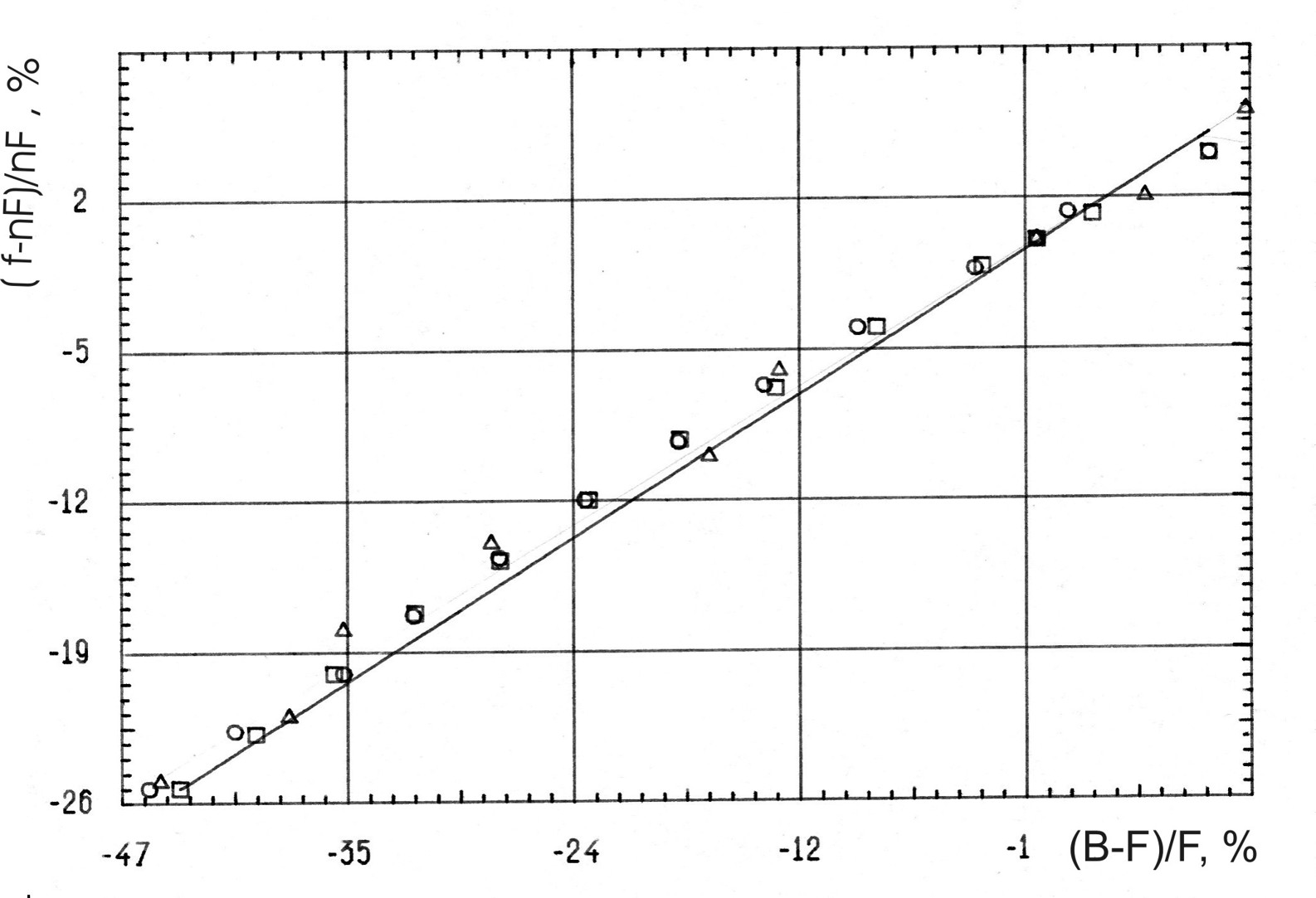
As for the frequency and focusing properties of diffractive elements using radiation
harmonics, their numeric and experimental analysis [1] revealed the following behaviour.
When an element operates on a harmonic, the frequency properties expressed in arbitrary
units are the same as the frequency properties of the diffractive element in the range of the
main wavelength (reference wavelength)– see fig. 3 (in this figure n is the number of the
frequency harmonic). This is also true for the transversal and longitudinal resolving powers
of a diffractive element if we appropriately replace the current (working) wavelength in the
expression.
Fig. 3. Frequency properties of a zone plate for the first three harmonics:
dnF=(f-nf0)/nf0
opensquaresn=1
open triangles n=2
open circles n=3
3.1 Chromatic confocal sensor
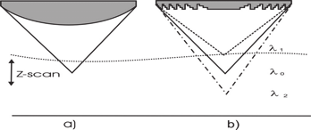
The frequency properties of a diffractive optics allow to modify, for example, a confocal
(multifocal) sensor [2]. Working principle of frequency-scanning confocal sensor
(microscopy) is as follows: the mechanical z-scan (Figure 4a) in conventional confocal
systems is replaced by a simultaneously generated series of foci at different wavelength
(Figure 4b).
This principle of frequency-scanning confocal microscopy may be applied at any frequency
waveband.
Diffractive Optics Microsensors
223
Fig. 4. Physical principle of frequency-scanning confocal sensor.
3.2 Wavefront sensor
Phenomena such as focusing or defocusing of a collimated beam by a lens and the free
propagation of a Gaussian beam can be well described as changes of the curvature of a
wavefront. The wavefront approach is also the most natural way of describing the operation of
optical elements made of a material with a spatially varying index of refraction. Wavefront
analysis is the enabling technology in the rapidly developing field of adaptive optics, etc. So
the concept of a wavefront is important in optics and in the physics of waves in general.
A Shack-Hartmann Wavefront Sensor is a device that uses the fact that light travels in a
straight line to measure the wavefront of light. The device consists of a lenslet array that
breaks an incoming beam into multiple focal spots falling on a optical detector. By sensing
the position of the focal spots the propagation vector of the sampled light can be calculated
for each lenslet. The wavefront can be reconstructed from these vectors. Shack-Hartmann
sensors have a finite dynamic range determined by the need to associate a specific focal spot
to the lenslet it represents.
One of the key problems with the development of a Shack-Hartmann wavefront sensor is
the fabrication of the lenslet array needed. The concept of using binary optics to fabricate
these arrays are perspective. The binary optics technique has proven to be successful and is
capable of making a large number of different devices with high fidelity.
The similar sensor may be used, for example, for flow measurements. One-dimensional
linear sensor arrays that are capable of measuring the phase of optical radiation after it has
propagated through the flow field are arranged on the opposite side. These wavefront
sensors measure the optical path errors induced on the laser beams by the density variations
in the flow caused by the mixture of heated air and entrained cooler room air in the jet.
Although each sensor array detects the path-integrated phase in a particular direction
through the flow, the set of sensor arrays collects information along many different
directions through the flow simultaneously, enabling the inversion ofthe data set and
yielding a detailed spatially resolved picture of the plane of the flow through which all the
lasers propagated. When the set of sensor arrays in this optical tomography system is
operated at speeds of several kilohertz, a tomographic movie of the flow structure in a 2D
plane of the flow can be obtained frame by frame [3].
3.3 Fresnel zone plate spectrometer.
DOE can be made to simultaneously disperse the wavelengths of the incoming light - like a
grating- at the same time they focus the energy. Figure 5 shows the set-up of Fresnel micro-
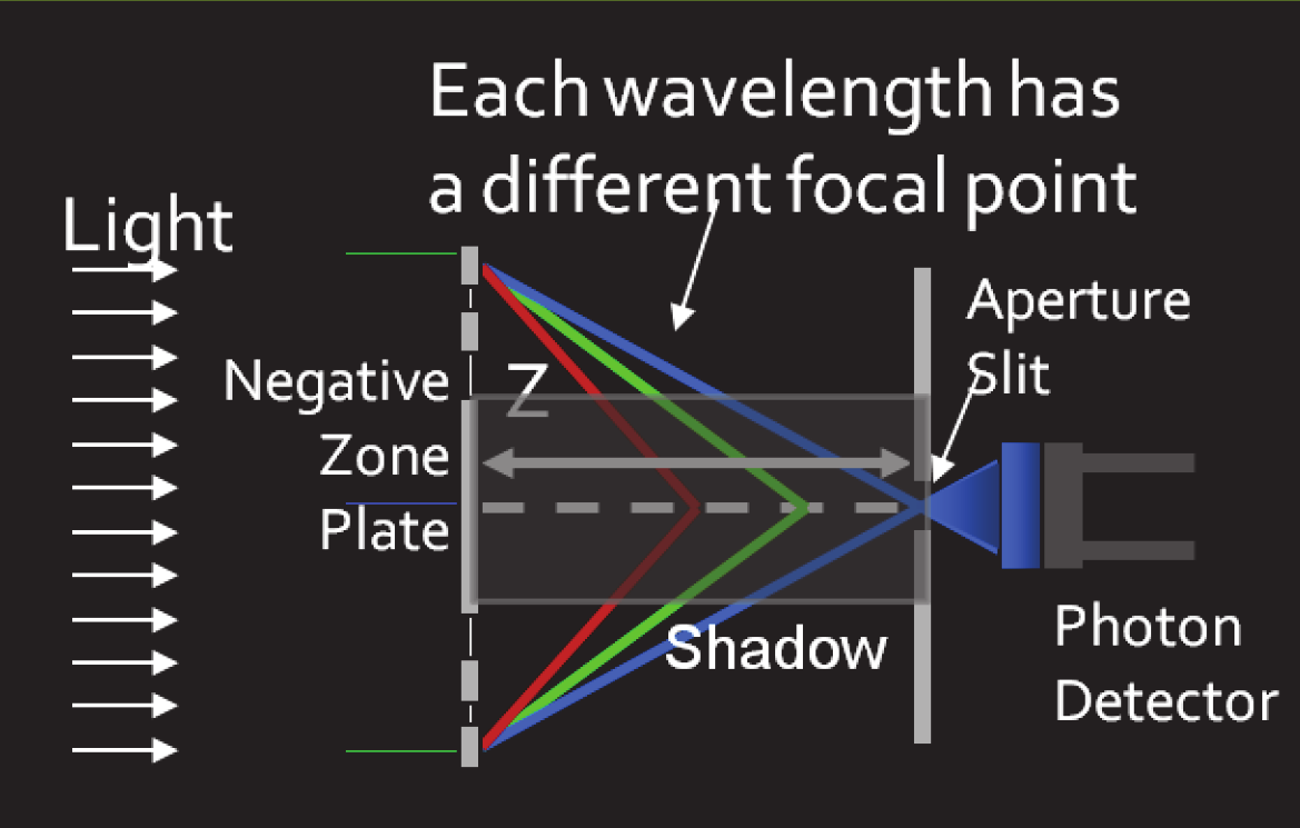
224
Microsensors
spectrometer with the opaque-center zone plate. A binary zone plate was typically designed
with a concentric series of transparent and opaque rings. It is very interesting to note that
when the radius of the zone plate is miniaturized by M times with a linear miniaturization factor M such that in paraxial approximation
K
K
n
r
n , the focal length becomes 2 ,
M
2
M
which is shortened by M 2 times. Therefore when the zone plate is miniaturized by five
times, the overall thickness due to the focal length is shortened by 25 times, thus
approaching a thin-film structure. The focusing properties of the “scaled” FZP is considered
in [1]. This miniaturization relation is valid in the Fresnel regime in paraxial approximation.
When the optical length Z is changed with a linear scanning actuator, the photon intensity at
the detector behind the round aperture slit is recorded with Z which corresponds to K2/ [4].
Fig. 5. Optical set-up diagram of a Fresnel micro-spectrometer with negative zone plate:
cross-sectional view [4].
The authors [4] have demonstrated that the spectral resolution and resolving power of an
ideal Fresnel micro-spectrometer do not depend on the miniaturized size but only on the
total number of rings in the Fresnel regime. This is analogous to the spectral resolution
relationship of a linear grating with Fraunhofer diffraction. The authors conclude that
further miniaturized and improved spectrometers based on Fresnel diffraction can be built if
the total number of rings is kept constant or increased.
Low-cost spectrometric sensors utilizes both the dispersing and the focusing abilities of
Fresnel zone-like diffractive structures [5]. The standard grating and collimating optics of a
scanning spectrometer are replaced with a dispersive and focusing element. At the detector
scan area the selected wavelength bands pass over the detector in a predetermined order
giving rise to peaks in the detector signal. A DOE may be designed to focus two or more
wavelength bands simultaneously onto the same detector position, and the power in the
bands may be weighted relative to each other.
Diffractive Optics Microsensors
225
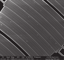
Reconfigurable components are well adapted to NIR spectroscopic sensors. In a feasibility
study a diffraction filter was fabricated in Si [6] that is both re-configurable and focuses the
light. It consists of an array of moveable segments of a Fresnel zone plate; each segment
having a few grating grooves (Fig. 6). Each segment is actuated vertically by electrostatic
parallel-plate actuators situated outside the optically active part.
Fig. 6. A micro-mechanical Fresnel lens with 14-segment (left) and a closer view at one
segment consisting of 7 grating grooves (right),as seen with a scanning electron microscope
[5-6].
In the idle mode the zone plate focuses a target wavelength at the detector. When every
other segment of the structure was pulled down, a destructive interference occurs at the
centre wavelength giving rise to a sideband on each side of the target wavelength. The
target wavelength represents e.g. the absorption line of a gas and will be measured in the
226
Microsensors
idle mode of the actuator, whereas in the activated mode the background on both sides of
the target line is measured.
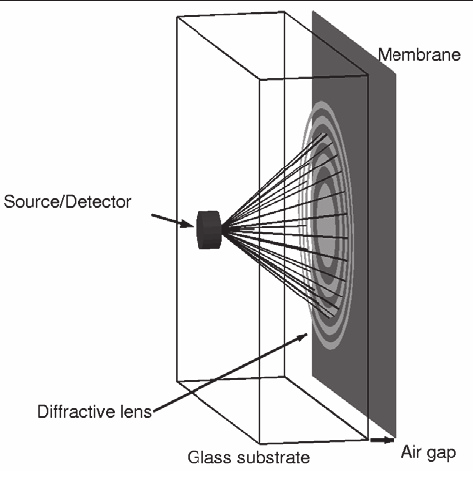
3.4 Diffractive optical microphone
Optical microphones are able to solve major problems that capacitive sensors are suffering
from. Optical sensors have no problems with high voltage biasing or need of electrical
isolation. They are able to achieve equal or better sensitivity than capacitive displacement
sensors with less demanding electronics. The authors describe a new approach where they
integrate a diffractive lens into the microphone transducer [7]. An optical microphone
consists of a membrane (based on diffractive optical element or Fresnel zone plate) that is
deflected by sound pressure or an acoustic signal, where the movement of the membrane is
measured by the change in transmitted light intensity due to diffraction. For a given
displacement Δ d of diffractive element surface we can maximize the change in measured optical
power, given by the change in diffraction efficiency. The lens consists of a metallic pattern
on the substrate, an air gap and a reflecting membrane as shown in Fig 7. The diffractive
lens allows to use a simple optical readout system with no additional collimating or
focusing optics.
Fig. 7. Simplified geometry of the diffractive microphone. The optical fiber may be replaced
by an LED source and a photodiode detector attached to the substrate [7].
By placing a source and detector in the focal plane of the diffractive lens, the measured
intensity will be highly sensitive to the position of the membrane.
The diffractive lens was a glass substrate with a 2mm 2mm chrome pattern in the form of a
diffractive lens. The authors believed that the microphone can be cheaper, smaller, and are
Diffractive Optics Microsensors
227
well suited for integrated design and mass production with photolithography. The
fiberbased diffractive lens microphone is suited for demanding applications such as nuclear
radiation, medicine and areas with danger of explosion.
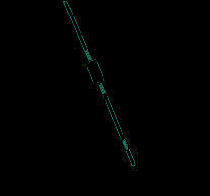
4. Diffractive optic fluid shear stress sensor [8]
Accurate measurement of the wall shear stress is needed for a number of aerodynamic
studies. Light scattering off particles flowing through a two-slit interference pattern can be
used to measure the shear stress of the fluid. The authors [8] designed and fabricated a
miniature diffractive optic sensor based on this principle. The developed sensor provided an
integrated diffractive optical element (DOE) sensor that integrated the transmitter and
receiver optics on the same substrate, as shown in Figure 8. The surface mounted sensor
generates a pattern of diverging interference fringes, originated at the surface, and extended
into the boundary layer region.
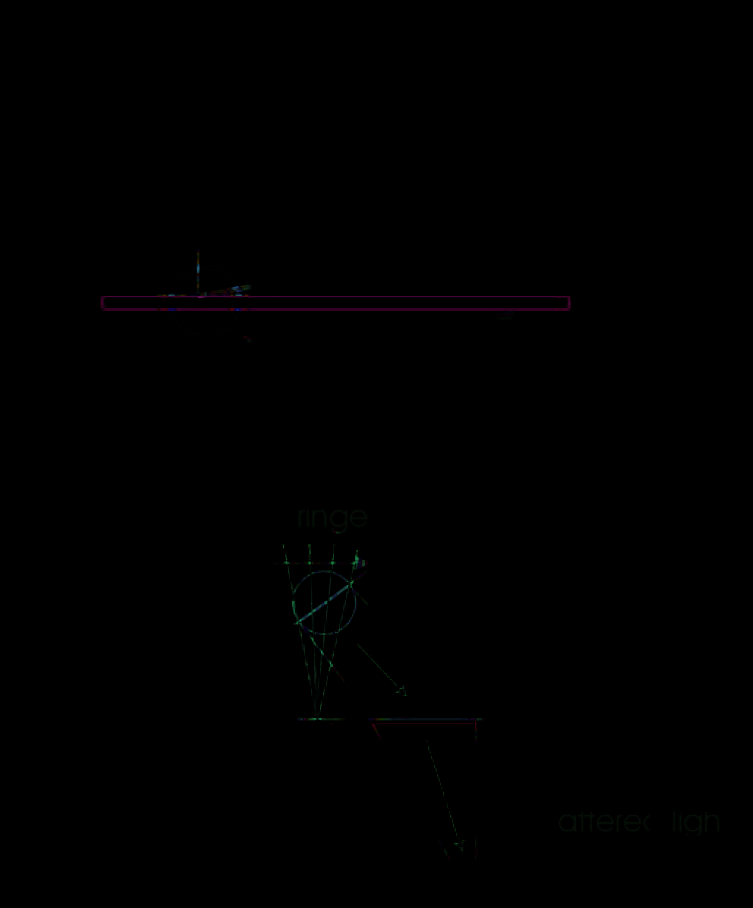
Fig. 8. Schematic of the Micro-shear stress sensor [8].
228
Microsensors
The intersection region of the transmission fringe pattern and the receiver field of view
defined by the backscatter collection optics defined the overall measurement volume
location and dimension.
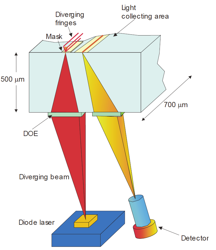
A conceptual drawing of the micro-shear stress sensor is shown in Figure 9. The diverging
light from a diode laser is focused by a DOE to two parallel line foci. These foci are
coincident with two slits in a metal mask on the opposite side of a quartz substrate. The
light diffracts from the slits and interferes to form linearly diverging fringes to a good
approximation. The light scattered by particles traveling through the fringe pattern is
collected through a window in the metal mask. Another DOE on the backside focuses the
light to an optical fiber connected to a detector.
Fig. 9. Schematic of the shear stress sensor assembly [8].
The main sensor element was fabricated by two-sided lithography on a 500 μm thick quartz
substrate. The slits and collecting window on the front were fabricated by direct-write
electron-beam lithography followed by wet etching of evaporated chrome. The polymethyl
methacrylate (PMMA) diffractive optical elements on the back were fabricated by analog
direct-write electron-beam lithography followed by acetone development [8].
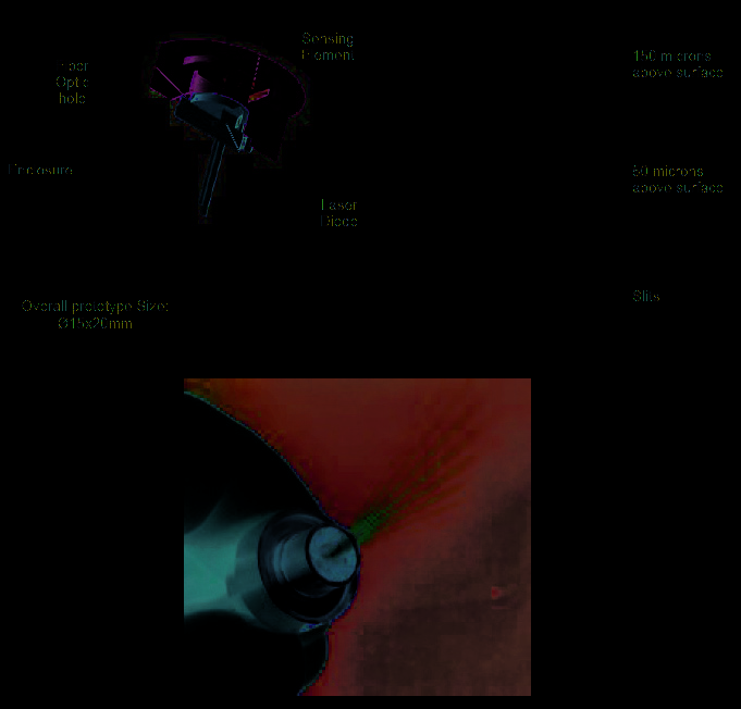
The shear stress sensor’s elements were assembled into a package (Fig. 10 left) with a diode
laser (660 nm) and a port for the collection fiber. The overall size of this prototype is 15 mm
in diameter and 20 mm in length. The fringes were imaged with a CCD camera using a
microscope objective and are shown in Fig. 10. The fringe divergence was measured to be
linear with a slope in close agreement with theory. The contrast is very satisfactory and
Diffractive Optics Microsensors
229
preliminary tests using a moving surface through the fringe pattern yield a clear signal.
Testing of the receiver side of the sensor element is underway.
A photograph of the shear stress sensor is shown in Figure 10 (bottom). The sensor
substrate, shown in, is mounted into the sensor element location shown on the front face of
the assembly. The diverging fringe pattern is visible away from the surface. In this
configuration, the light source and the detection electronics are located remotely and are
connected to the sensor through optical fibers.
Fig. 10. Shear stress sensor assembly (left) and photographs of the fringes at different
heights above the surface (right). Micro-optical shear stress sensor is shown in bottom [8].
4.1 Remote point diffractive optical sensors
The ever-increasing need for sensing in the chemical and physical domain has led to the
development of a variety of sensing schemes, including electrochemical and optical sensors.
Alternative optical sensing methods use a remotely transmitted light beam to interact with a
lossless material exposed to an analyte. A laser beam propagates in free space (or in optical
waveguides/fibers), and by interrogating a suitable nanocomposite medium, the “sensor
head,” it becomes modulated, thus producing the sensor signal. The sensor head is a
230
Microsensors
powerless (electrically passive) thin-film device of the environmentally sensitive material,
not electrically connected to any power or signal processing unit. In a diffractive device, the
environmentally induced changes of the optical properties are translated to measureable
alterations of the transmitted/reflected diffracted beams. A diffractive NiCl2 /SiO2
nanocomposite photonic sensor for ammonia was demonstrated in [9]. The device has been
fabricated on a thin-film structure using direct UV laser microetching techniques. The first-
order diffracted beams were found to provide an appreciable sensor response at SNR ~ 18.6,
which allowed the detection of quite low, 2 ppm, ammonia levels.
An optimization study of surface relief grating based sensors for use in diffractive optical
remote point sensing was presented in [10].
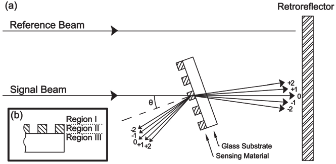
Fig. 11. Remote point sensing by the diffractive device. (a) Schematic overview and (b) SRG
geometry used for theory and design [10].
The RPS concept is schematically depicted in figure 11. The passive sensor head consists of a
sensing material thin film deposited on a glass substrate. The sensing material is designed to
reversibly alter its optical properties upon exposure to a chemical or physical agent. The
sensor head is placed in the area to be monitored and it is remotely interrogated in real time
by measuring the reflected signal beam. DOEs and photonic