L6
L6
L5
L1
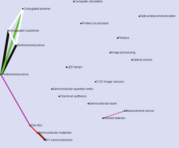
Fig. 9. Cluster map of P1 (2000-2004), with indication of the strength of the connections
L1
L6
L6
L3
L4
L5
L5
L6
L6
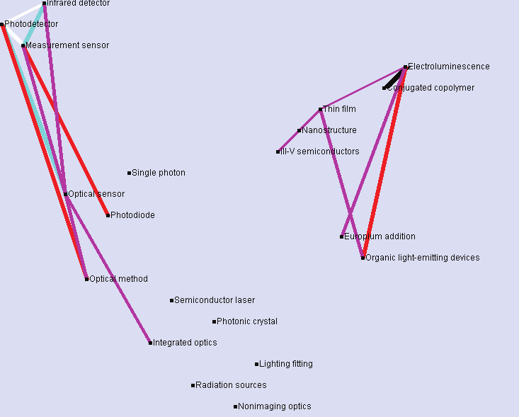
Fig. 10. Cluster map of P2 (2005-2010), with indication of the strength of the connections
In both maps produced by Stanalyst, each dot corresponds to a cluster and each line gives
the connexion level between pairs of clusters. Note that we considered here only the 6
144
Optoelectronic Devices and Properties
highest levels (out of the 10 defined by the connected component analysis step)
corresponding to the strongest connexions between clusters.
In Stanalyst, the level of connexions is code-coloured. Since these colours do not come out in
print, we mentioned in figure 9 and 10 the level next to the connexion with a symbols going
from L1 (strongest connection) to L8 (weakest connection).
4.2.2 Comparison matrix analysis
The main purpose of the diachronic cluster analysis is to determine which topics of the
second period find their roots in the first one and which new topics emerge in the second
period. In order to analyze the evolution of the cluster vocabulary between the two
considered periods, we built a comparison matrix pointing out the percent of keywords
belonging to the second-period clusters and already existing in the first-period clusters. The
cumulated percentage is also calculated for each second-period cluster. Using this matrix,
we can identify different cluster behaviours: stability, fusion or splitting. Using the cluster
maps, we can also detect status change of the clusters in the global network.
The comparison matrix is showed in table 12. For instance, if we consider the row 17 of the
matrix, corresponding to the cluster “Nanostructure” of P2, we can see that 26% (see
element highlighted) of its keywords come from the cluster “Chemical synthesis” (see
column 4) of P1. Furthermore, the cumulated values of the set of inheritances of each cluster
of P2, in terms of keywords already present in the clusters of P1, are given in the marginal
column.
P2/P1 1 2 3 4 5 6 7 8 9 10 11 12 13 14 15 16 17 18 19 20
1
3 0 3 7 0 0 0 0 0 7 22 0 0 0 3 7 7 0 7 0 66
2
0 42 4 0 0 4 0 0 0 0 0 4 0 0 0 0 0 9 0 0 63
3
0 0 0 4 2 0 24 0 0 21 4 0 26 0 0 34 0 0 7 0 122
4
2 6 2 2 0 4 0 2 6 0 0 2 0 2 4 0 4 0 0 0 36
5
3 1 8 2 0 0 0 1 0 0 0 3 0 3 2 0 2 7 5 12 49
6
4 1 8 5 0 0 0 0 0 0 0 5 0 2 2 0 1 8 1 11 48
7
8 5 1 0 3 5 0 0 3 0 0 1 0 3 7 0 26 0 1 3 66
8
0 0 0 12 4 5 4 0 5 4 31 0 4 0 5 5 0 1 1 0 81
9
2 0 11 0 0 0 0 3 0 0 0 6 0 5 1 0 0 4 7 3 42
10
1 0 5 0 0 0 0 2 0 1 0 1 2 4 0 1 2 4 51 4 78
11
0 7 2 7 11 33 4 0 40 2 14 0 4 0 0 4 7 0 0 0 135
12
0 0 0 0 2 0 13 0 0 5 2 0 73 0 0 15 0 0 5 0 115
13
2 10 2 0 0 0 0 2 0 0 5 5 0 2 0 0 0 18 0 7 53
14
12 0 4 0 0 1 0 6 0 0 0 1 0 7 9 0 11 3 0 12 66
15
8 1 4 1 1 0 0 2 1 0 4 1 0 7 15 0 7 0 2 3 57
16
5 0 8 5 4 0 0 7 0 0 0 0 0 5 8 0 7 1 7 7 64
17
1 1 3 26 1 1 5 0 1 1 9 1 5 0 5 5 1 0 0 1 67
18
1 0 1 10 0 7 1 0 0 1 12 3 1 1 3 3 1 0 9 0 54
19
4 1 4 3 0 1 0 3 1 0 1 9 0 5 3 0 1 12 4 5 57
20
4 13 0 0 4 9 0 0 4 0 4 13 0 9 13 0 9 13 0 4 99
Table 12. Comparison matrix of the keywords of the two periods: P1 (2000-2004) and P2
(2005-2010)
Identification of Emergent Research Issues:the Case of Optoelectronic Devices
145
The analysis of the comparison matrix allows us to singularize in the second period (see
table 13):
•
eight homonymous clusters, but only four of them seem to be stable
•
three clusters with new titles but presenting characteristics of stability
•
four clusters with a low (less than 50%) inheritance global rate from the clusters of P1 -
Are they new clusters?
•
three clusters with a strong (more than 100%) inheritance global rate from different
clusters of P1 – Do they convey “old”, already known information?
Type of singularization
Cluster name
Homonymy with P1, apparent stability
Infrared detector, Semiconductor laser,
(larger keywords inheritance coming from
Thin film, Conjugated copolymer
the homonymous cluster of P1)
Homonymy with P1, less apparent stability Electroluminescence, Optical sensor, III-V
(larger keywords inheritance coming from
semiconductors, Measurement sensor
other clusters of P1 than the homonymous
one)
New title with stability characteristics Organic
light-emitting devices, Lighting
fitting, Nanostructure
Low inheritance global rate
Single photon, Nonimaging optics, Optical
sensor, Optical method
High inheritance global rate
III-V semiconductors, Conjugated
copolymer, Electroluminescence
Table 13. Clusters singularized in second period
4.2.3 Experts validation
Starting from these quantitative data the expert worked on the validation of our hypotheses
by analysing the contents of the clusters and their relative position in the cluster network
drew in the map of each period. Special attention has been paid on the detection of brutal
changes of cluster relative position.
The expert’s analysis confirms the stability of two homonymous clusters between P1 and P2:
“Infrared detector” and “Semiconductor laser”. The homonymous clusters “Thin film” and
“Conjugated copolymer” are rather stable between P1 and P2, but the former shows a
higher relative weight of organic towards inorganic materials in P2, and the latter a higher
relative weight of devices towards characterization of the materials.
Despite their less apparent stability, due to a lower inheritance from P1 to P2, the
homonymous clusters “Measurement sensor” and “III-V semiconductors” are stable
between P1 and P2. The other clusters of P1 from which they inherit deal with similar
topics.
The P2 cluster “Optical sensor” does not inherit predominantly from its P1 homonymous.
Meanwhile, its stronger keywords inheritance comes from topically close clusters as “Image
processing” and “Measurement sensors”. This cluster is rather stable between P1 and P2,
but it highlights the emergence in P2 of some applications related to biomedical imaging
and security. The take off of these new applications of sensors can explain the relatively low
inheritance level of the P2 clusters “Optical sensor” and “Optical method”.
146
Optoelectronic Devices and Properties
As the former one, the P2 cluster “Electroluminescence” does not inherit predominantly
from its P1 homonymous. Indeed, three P1 clusters hand more keywords down to it than its
homonymous: “Photoluminescence”, “Conjugated polymers” and “Conjugated
copolymers”. This fact shows the strong inheritance relation between the studies of P1
related to synthesis of conjugated (co)polymers and characterization of their luminescent
properties, and the studies of P2 related to the potential applications of these materials for
the design of electroluminescent devices.
The strong inheritance of the P2 cluster “Lighting fitting” from the P1 cluster “LED lamps”
shows the importance of the topic dealing with the use of electroluminescent devices as light
sources through the two periods of time. In the second period, the weight of this topic is
reinforced by the presence of the cluster “Nonimaging optics” and by a growing number of
bibliographic records.
The P2 cluster “Organic light-emitting devices” inherits most of its keywords from the P1
cluster “Thin films”. This relation shows the temporal evolution of the field, from the study
of the potential use of thin films and heterostructures in optoelectronic devices in P1, to the
fabrication and characterization of these devices in P2. The stronger implication of organic
materials in P2, highlighted by the name of the P2 cluster, confirms the tendency formerly
observed when analyzing the stability of the homonymous class “Thin films” between P1
and P2.
The P2 cluster “Nanostructure” inherits most of its keywords from the P1 cluster “Chemical
synthesis”, which deals essentially with the synthesis of nanomaterials (nanowires,
nanocomposites, nanoboxes, nanospheres…). This inheritance, together with the strong
relative growth of the number of documents between the two clusters, shows the growing
importance of nanomaterials in the field of optoelectronic devices in P2.
Amongst the clusters of P2 showing a low marginal value, “Single photon” gathers
bibliographic records dealings with the application of avalanche photodiodes to fields like
quantum information, quantum communication or quantum cryptography. This low
marginal value is thus closely related to the emergence of a new scientific field.
The analysis of the cluster maps obtained for the two periods completes and confirms these
observations.
In the cluster map of the first period (see figure 11), the four cluster “Conjugated polymers”,
“Conjugated copolymers”, “Electroluminescence” and “Photoluminescence” form a very
strong network (N1), This result highlights the importance of organic semiconductors in the
field of optoelectronic devices and confirms the conclusion of a former study, in which we
analyzed the evolution of the same scientific field over an older time period (Schiebel et al.
2009). This network is still present in the second period, but it has included the cluster
“Organic light-emitting device”, illustrating the transition from materials to devices.
Furthermore, the proximity of the cluster “Nanostructure” shows the growing implication
of such materials in optoelectronic devices in P2.
The topic related to imaging devices is already present in the first period (see figure 11), but
the corresponding clusters (“Measurement sensor”, “Infrared detector”, “Optical sensor”,
“Image processing”) do not show strong relations. On the contrary, they form a much strong
network (N2) in the second period (see figure 12). Though this topic is not new, the
comparison of the two cluster maps give evidence of its growing importance in the second
period. Close to this network, the appearance in the second period of the cluster “Single
photon” illustrates the emergence of quantum information processing in the field.
Identification of Emergent Research Issues:the Case of Optoelectronic Devices
147
N1
N2
Fig. 11. Networks of clusters for P1
N2
N1
Fig. 12. Networks of clusters for P2
Now we study the complementarity of both methodologies by comparing their results.
148
Optoelectronic Devices and Properties
5. Convergence between the two methodologies
Once applied to a corpus of 8,169 PASCAL bibliographic records related to optoelectronic
devices and divided into two successive periods (2000 to 2004 and 2005 to 2010), both
methodologies lead to complementary and converging results.
The stability of inorganic semiconductor materials over the two periods is illustrated by the
crossover from the stage “established term” to the stage “cross-section terms” (Pathway V)
of keywords like “III-V semiconductors” or “Gallium arsenides” (diffusion model) and by the
diachronic stability of the cluster “III-V semiconductors” (cluster analysis).
The leading role of organic materials, and especially organic polymers, over the two periods
is highlighted by the presence of keywords like “Conjugated copolymer”, “Conjugated polymer”
or “Phenylenevinylene derivative polymer” in the “established terms” and “cross-section terms”
stages of both periods (diffusion model) and by the strength of the cluster subnetwork N1
right from the first period (cluster analysis).
The growing importance of nanotechnology and nanomaterials in P2 is highlighted by the
crossover from the stage “unusual term” to the stage “cross-section terms” (Pathway III) of
the keyword “Nanoparticle” (diffusion model) and by the emergent role of cluster
“Nanostructure” in the second period map (cluster analysis).
The growing importance of imaging devices in P2 is highlighted by the crossover from the
stage “unusual term” to the stage “cross-section terms” (Pathway III) of the keyword
“Imager” (diffusion model) and by the strength of the cluster subnetwork N2 in the second
period map (cluster analysis).
The emergence in the second period of applications of optical sensors towards biomedical
imaging, highlighted by cluster analysis, is illustrated by the appearance of the keyword
“Biomedical imaging” amongst the top 10 “unusual terms” of the diffusion model in P2.
The reinforcement of the applications of LED as light sources, highlighted by cluster
analysis, is illustrated by the appearance of the keyword “Daylight” amongst the top 10
“unusual terms” of the diffusion model in P2. This keyword is related to studies focused on
the design of daylight emitting LED lamps.
6. Conclusion
It is a challenge to identify emerging technologies. “Optoelectronic devices” is a broad field
and by applying the complementary methods presented here, it can be better characterised
and described.
One particularity of our approach is the alternate utilisation of different bibliometric and/or
informetric methods and scientific expertise. This expertise is necessary to validate or to
complete the results obtained at each step of the work as well as to get the experts personal
input on the matter at hand. This could be time consuming, but with our approach, the
amount of data submitted to the experts’ appreciation is limited, thus making their task
notably easier.
The diachronic approach we adopted consists in splitting the corpus in two periods,
applying on the one hand the diffusion model to explore the terminological evolution of the
subject field, and on the other hand a content cluster analysis for each period to detect the
evolution of the topics by examination of the vocabulary related to the respective clusters.
The application of the diffusion model is a novel bibliometric approach giving a more in-
depth view of the considered field. Associating terms with technologies allows the
Identification of Emergent Research Issues:the Case of Optoelectronic Devices
149
development of a new interesting analysis methodology based on the notion of terminology
diffusion. The indicators we used such as term frequency, relative term frequency and age
of terms helped work out the different features of a field. Exploiting these results, we were
able to understand the field specifications. The bibliometric filter assigning keywords to
three stages gives an insight on the emergence of research topics in a technology. At a first
glance it is a formal taxonomy used to disassemble what is called a technology in its
“atoms” of research and traces the breakthroughs if they happen. Terms in the unusual
phase show potentials of future developments in a technology although it is neither a
prognosis, nor a prediction. To discuss the merit of emergences and research potentialities it
is important to obtain a validation of the results from experts in the concerned field.
Our cluster analysis approach allows to have a global view of the field landscape at two
successive time periods. The analysis of the cluster contents and their relative position on
the cluster maps supplies indications about their similarity with respect to their respective
associated keywords. The observation of cluster maps allows to detect exceptional topics
and interesting topic sub-sets. Here also, the experts’ input remains at each step absolutely
necessary to validate and position the analysis results in the field context by giving them a
scientific foundation.
Applying at the same time cluster analysis and diffusion model allows to confirm the results
detected by each method and also to lead to a deeper understanding and characterization of
the technological field. Furthermore, the diffusion model approach allows new
interpretation of clustering results introducing external term categorizations.
7. Acknowledgement
This work was carried out thanks to a European Union funding: Project number 15615 NEST
Programme launched within the framework of the 6th Research and Development
Framework Plan. The project acronym was PROMTECH and the project full title was
“Identification and Assessment of Promising and Emerging Technological Fields in
Europe”. The Consortium was composed by the Austrian Institute of Technology GmbH
(AIT, Vienna, Austria), the Fraunhofer Institut für Systemtechnik und Innovationsforschung
(ISI, Karlsruhe, Germany) and the Institut de l’Information Scientifique et Technique (INIST-
CNRS, Vandœuvre-lès-Nancy, France).
8. References
Armstrong, J. S., Green, K. C. (2007):
http://www.forecastingprinciples.com/selection_tree.html
Besagni D., François C., Hörlesberger M., Roche I. & Schiebel E. (2009): Les émergences
technologiques dans le domaine des dispositifs optoélectroniques : identification et
caractérisation, paper presented at the wokshop VSST (Veille Stratégique Scientifique
et Économique), 30-31 mars 2009, Nancy.
Kopcsa A. & Schiebel E. (1998): Science and technology mapping. A new iteration model for
representing multidimensional relationships. Journal of the American Society for
Information Science, 49 (1), 7–17.
Lancaster F. W. & Lee J. L. (1985): Bibliometric techniques applied to issues management: A
case study. Journal of the American Society for Information Science, 36(8), 389–397.
150
Optoelectronic Devices and Properties
Lelu A. (1993): Modèles neuronaux pour l’analyse de données documentaires et textuelles.
PhD Dissertation, Université de Paris 6.
Lelu A. & François C. (1992): Hypertext paradigm in the field of information retrieval: A
neural approach. 4th ACM conference on hypertext, Milano, November 30th–
December 4th.
PROMTECH (2007): Identification and Assessment of Promising Emerging Technological
Fields in Europe. Final report, July 2007, AIT, Vienna.
Roche I., Besagni D., François C., Hörlesberger M. & Schiebel E. (2010): Identification and
characterisation of technological topics in the field of Molecular Biology.
Scientometrics, 82(3), 663-676.
Schiebel E., Hörlesberger M., Roche I., François C. & Besagni D. (2009): An advanced
diffusion model to identify emergent research issues: the case of optoelectronic
devices . 12th International Conference on Scientometrics and Infometrics, ISSI 2009, July
14th-17th, 2009, Rio de Janeiro, Brazil.
Schiebel E., Hörlesberger M., Holste, D. Roche I., François C. & Besagni D. (2010):
Identification of emerging technologies through pathway-III analysis, Proceedings of
the 19th International Conference on Management of Technology. Cairo, Egypt, March
8th-12th, 2010
Schiebel E., Hörlesberger M., Roche I., François C. & Besagni D. (2010): An advanced
diffusion model to identify emergent research issues: the case of optoelectronic
devices. Scientometrics, 83(3), 765-781.
8
Synchronous Vapor-Phase Coating of
Conducting Polymers for Flexible
Optoelectronic Applications
Keon-Soo Jang and Jae-Do Nam
Sungkyunkwan University
Republic of Korea
1. Introduction
Since conducting polymers (CP) were first reported, poly(3,4-ethylenedioxythiophene)
(PEDOT) is arguably one of the most commercially useful and most studied CPs in the last
20 years (Shirakawa et all., 1977; Chiang et al., 1977; Winther-Jensen et al., 2007; Truong et
al., 2007) . PEDOT has been studied extensively on account of its many advantageous
properties, such as high electrical conductivity, good transmittance and thermal stability
with a low optical bandgap and thermal stability (Winther-Jensen & West, 2004; Jonas et al.,
1991). These properties make PEDOT very attractive for applications, such as electrochromic
windows (Welsh et al., 1999), organic electrodes for organic photovoltaic cells (OPVs)
(Admassie et al., 2006; Gadisa et al., 2006) and hole injection layers (HIL) in organic light
emitting devices (OLEDs) (Wakizaka et al., 2004; Hatton et al., 2009) and dye-sensitized
solar cells (Saito et al., 2005). In particular, PEDOT is commonly used as a hole extraction
layer in OPVs (Colladet et al., 2007; Kim et al., 2005). In most optoelectronic applications as a
buffer or electrode layer, the bandgap of the layer plays an important role in determining
the operating characteristics, quantum efficiency and electron/hole transport. Therefore, the
main issues for electronic device applications include both the electrical conductivity and
bandgap.
Oxidized PEDOT can be produced in a variety of forms using different polymerization
techniques. Solution processing is used most commonly in synthesizing PEDOT in the form
of spin-coating, solvent-casting or ink-jet printing. However, these PEDOT systems are
relatively insoluble in most solvents, making it necessary to attach soluble functional groups
to the polymer or dope it with stabilizing polyelectrolytes (Terje & Skotheim, 1998). An
aqueous dispersion of poly(3,4-ethylenedioxythiophene)-poly(styrenesulfonate) (PEDOT-
PSS), commercially available as Baytron P, is a stable polymer system with a high
transparency up to 80% (Groenendaal et al., 2000). However, the PEDOT-PSS film exhibits
relatively low electrical conductivity, 10-500 S/cm (Groenendaal et al., 2000), which does not
often meet the high conductivity required for most applications. In addition, scanning-
tunneling microscopy, neutron reflectivity measurements, and x-ray photoelectron
spectroscopy have revealed a PSS rich layer on the top of the spin-coated PEDOT-PSS films
due to the phase separation (Lee & Chung, 2008; Kemerink e