ethylenedioxythiophene) and Its Derivatives: Past, Present, and Future Adv. Mater.
12, 481-494.
Groenendaal, L.; Zotti, G.; Jonas, G. (2001). Optical, conductive and magnetic properties of
electrochemically prepared alkylated poly(3,4-ethylenedioxythiophene)s Synthetic
Met. 118, 105-109.
Ha, Y.; Nikolov, N.; Pollack, S.; Mastrangelo, J.; Martin, B.; Shashidhar, R. (2004). Towards a
Transparent, Highly Conductive Poly(3,4-ethylenedioxythiophene) Adv. Funct.
Mater. 14, 615-622.
Hatton, R.; Blanchard, N.; Tan, L.; Latini, G.; Cacialli, F.; Silva, S. (2009). Oxidised carbon
nanotubes as solution processable, high work function hole-extraction layers for
organic solar cells Org. Electron. 10, 388-395.
Higgins, A.; Martin, S.; Jukes, P.; Geoghegan, M.; Jones, R.; Langridge, S.; Cubitt, R.;
Kirchmeyer, S.; Wehrum, A.; Grizzi, I. (2003). Interfacial structure in
semiconducting polymer devices J. Mater. Chem. 13, 2814-2818.
Holdcroft, S. J. (1991). Determination of molecular weights and Mark–Houwink constants
for soluble electronically conducting polymers Polym. Sci., Part B. 29, 1585.
Jang, K.; Eom, Y.; Lee, T.; Kim, D.; Oh, Y.; Jung, H.; Nam, J. (2009). Fabrication of Poly(3-
hexylthiophene) Thin Films by Vapor-Phase Polymerization for Optoelectronic
Device Applications ACS Appl. Mater. Interfaces 1, 1567-1571.
Jang, K.; Kim, D.; Lee, J.; Hong, S.; Lee, T.; Lee, Y.; Nam, J. (2010). Synchronous vapor-phase
polymerization of poly(3,4-ethylenedioxythiophene) and poly(3-hexylthiophene)
copolymer systems for tunable optoelectronic properties Org. Electron. 11, 1668-
1675.
Johansson, E. & Larsson, S. (2004). Electronic structure and mechanism for conductivity in
thiophene oligomers and regioregular polymer Synthetic Met. 144, 183
Jonas, F.; Schrader, L. (1991). Conductive modifications of polymers with polypyrroles and
polythiophenes Synthetic Met. 41, 831-836.
Kemerink, M.; Timpanaro, S.; De Kok, M.; Meulenkamp, E.; Touwslager, F. (2004). Three-
Dimensional Inhomogeneities in PEDOT:PSS Films J. Phys. Chem. B 108, 18820-
18825.
Kim, D.; Lee, L.; Kang, S.; Jang, K.; Lee, J.; Cho, M.; Nam, J. (2009). In-situ blends of
polypyrrole/poly(3,4-ethylenedioxythiopene) using vapor phase polymerization
technique Thin Solid Films 517, 4156-4160.
Kim, J.; Kim, E.; Won, Y.; Lee, H.; Suh, K. (2003). The preparation and characteristics of
conductive poly(3,4-ethylenedioxythiophene) thin film by vapor-phase
polymerization Synthetic Met. 139, 485-489.
Kim, Y.; Choulis, S.; Nelson, J.; Bradley, D.; Cook, S.; Durrant, J. (2005). Device annealing
effect in organic solar cells with blends of regioregular poly(3-hexylthiophene) and
soluble fullerene Appl. Phys. Lett. 86, 063502.
Lee, T. & Chung, Y. (2008). Control of the Surface Composition of a Conducting-Polymer
Complex Film to Tune the Work Function Adv. Funct. Mater. 18, 2246-2252.
Lee, T.; Chung, Y.; Kwon, O.; Park, J. (2007). Self-Organized Gradient Hole Injection to
Improve the Performance of Polymer Electroluminescent Devices Adv. Funct. Mater.
17, 390-396.
Levenspiel, O. (1962). Chemical reaction engineering, John Wiley and Sons, New York, 1962
Synchronous Vapor-Phase Coating of Conducting Polymers
for Flexible Optoelectronic Applications
169
Li, L.; Huang, Y.; Yan, G.; Liu, F.; Huang, Z.; Ma, Z. (2009). Poly(3,4-
ethylenedioxythiophene) nanospheres synthesized in magnetic ionic liquid Mater.
Lett. 63, 8-10.
Li, Z. L.; Yang, S. C.; Meng, H. F.; Chen, Y. S.; Yang, Y. Z.; Liu, C. H.; Horng, S. F.; Hsu, C. S.;
Chen, L. C.; Hu, J. P. (2004). Patterning-free integration of polymer light-emitting
diode and polymer transistor Appl. Phys. Lett. 84, 3558
Liu, J.; Loewe, R. S.; McCullough, R. D. (1999). Employing MALDI-MS on
Poly(alkylthiophenes): Analysis of Molecular Weights, Molecular Weight
Distributions, End-Group Structures, and End-Group Modifications Macromolecules
32, 5777
McCullough, R. D. (1998). The Chemistry of Conducting Polythiophenes Adv. Mat. 10, 93.
Perepichka, I. F.; Perepichka, D. F.; Meng, H.; Wudl, F. (2005). Light-Emitting
Polythiophenes Adv. Mat. 17, 2281.
Saito, Y.; Kitamura, T.; Wada, Y.; Yanagida, S. (2002). Poly(3,4-ethylenedioxythiophene) as a
hole conductor in solid state dye sensitized solar cells Synthetic Met. 131, 185-187.
Sarac, A.; Sonmez, G.; Cebeci, F. (2003). Electrochemical synthesis and structural studies of
polypyrroles, poly(3,4-ethylene-dioxythiophene)s and copolymers of pyrrole and
3,4-ethylenedioxythiophene on carbon fibre microelectrodes J. Appl. Electrochem. 33,
295-301.
Shirakawa, H.; Louis E.; MacDiarmid, A.; Chiang, C.; Heeger, A. (1977). Synthesis of
electrically conducting organic polymers: halogen derivatives of polyacetylene,
(CH)x J. S. C., Chem. Commun. 1977, 578-580
Singh, R.; Kumar, J.; Singh, R.; Kant, R.; Chand, S.; Kumar, V. (2007). Micromorphology,
photophysical and electrical properties of pristine and ferric chloride doped poly(3-
hexylthiophene) films Mater. Chem. Phys. 104, 390-396.
Skotheim, T. A.; Reynolds, J. R. Eds.; Handbook of conducting polymers, CRS press 2007.
Terje A. Skotheim, Handbook of Conducting Polymer Marcel Dekker, New york, 1998.
Truong, T.; Kim, D.; Lee, Y.; Lee, T.; Park, J.; Pu, L.; Nam, J. (2008). Surface smoothness and
conductivity control of vapor-phase polymerized poly(3,4-ethylenedioxythiophene)
thin coating for flexible optoelectronic applications Thin Solid Films 516, 6020-6027.
Wakizaka, D.; Fushimi, T.; Ohkita, H.; Ito, S. (2004). Hole transport in conducting ultrathin
films of PEDOT/PSS prepared by layer-by-layer deposition technique Polymer 45,
8561-8565.
Welsh, D.; Kumar, A.; Meijer, E.; Reynolds, J. (1999). Enhanced Contrast Ratios and Rapid
Switching in Electrochromics Based on Poly(3,4-propylenedioxythiophene)
Derivatives Adv. Mater. 11. 1379-1382.
Winther-Jensen, B.; Chen, J.; West, K.; Wallace, G. (2004). Vapor Phase Polymerization of
Pyrrole and Thiophene Using Iron(III) Sulfonates as Oxidizing Agents
Macromolecules 37, 5930.
Winther-Jensen, B.; Chen, J.; West, K.; Wallaces, G. (2004). Vapor Phase Polymerization of
Pyrrole and Thiophene Using Iron(III) Sulfonates as Oxidizing Agents
Macromolecules 37, 5930-5935.
Winther-Jensen, B.; Forsyth, M.; West, K.; Andreasen, J.; Wallace, G.; MacFarlane, D. (2007).
High current density and drift velocity in templated conducting polymers Org.
Electron. 8, 796-800.
170
Optoelectronic Devices and Properties
Winther-Jensen, B.; West, K. (2004). Vapor-Phase Polymerization of 3,4-
Ethylenedioxythiophene: A Route to Highly Conducting Polymer Surface Layers
Macromolecules 37, 4538-4543.
Xu, J.; Wang, J.; Mitchell, M.; Mukherjee, P.; Jeffries-EL, M.; Petrich, J. W.; Lin, Z. (2007).
Organic−Inorganic Nanocomposites via Directly Grafting Conjugated Polymers
onto Quantum Dots J. Am. Chem. Soc. 129, 12828
Xu, Y.; Wang, J.; Sun, W.; Wang, S. (2006). Capacitance properties of poly(3,4-
ethylenedioxythiophene)/polypyrrole composites J. Power Sources 159, 370-373.
Zhan, L.; Song, Z.; Zhang, J.; Tang, J.; Zhan, H.; Zhou, Y.; Zhan, C. (2008). PEDOT: Cathode
active material with high specific capacity in novel electrolyte system Electrochim.
Acta 53, 8319-8323.
Part 2
Nanostructures:
Properties and Applications
9
ZnO Nanostructures
for Optoelectronic Applications
Ashok K. Sood1, Zhong Lin Wang2, Dennis L. Polla3, Nibir K. Dhar3,
Tariq Manzur4 and A.F.M. Anwar5
1Magnolia Optical Technologies Inc, 52-B Cummings Park, Suite 314,
Woburn, MA 01801
2School of Materials Science and Engineering, Georgia Institute of Technology,
771 Ferst Drive, Atlanta, GA 30332
3DARPA/MTO, 3701 North Fairfax Drive, Arlington, VA 22203
4Naval Underwater Warfare Center, 1176 Howell Street, Newport, RI 02841
5Department of Electrical Engineering, University of Connecticut, Storrs, CT 06269
U.S.A.
1. Introduction
ZnO is a unique material that exhibits both semiconducting and piezoelectric properties.
ZnO is a unique material that exhibits both Semi conducting and piezoelectric properties.
ZnO devices have been demonstrated for applications in piezoelectric pressure sensors and
Pyroelectric infrared detectors [1] and Spintronic devices [2]. More recently, there has been
significant effort underway for design and development of ZnO nanostructures such as ZnO
nanowires for a variety of applications [3-7].
The ZnO nanostructures can be implemented in Optoelectronic, Sensors, Transducers and
Biomedical applications [1, 2, 3, 4]. Use of these nanostructures, will allow building of
Nanoscale nanosensors, nanocantilevers, field-effect transistors and nanoresonators for a
variety of Military, Homeland Security and Commercial Applications. Due to the
advancement of materials technology over the past decade, wide-band gap semiconductors
such as SiC, GaN and ZnO have emerged as UV sensitive materials that have applications
for UV lasers, UV Photodetector, switches, Bio-Sensors and solar cells.
ZnO wide-band gap semiconductor is promising for sensor applications in the UV range.
The band-gap is 3.2 eV for ZnO. Therefore, GaN and ZnO, as well as SiC are potentially
good materials to cover the UV spectral band (240-280 nm), when solar radiation is
completely absorbed by the ozone layer of the earth atmosphere, so the background of solar
radiation at the earth surface is essentially zero.
ZnO is transparent to visible light and can be made highly conductive by doping. ZnO is a
versatile functional material that has a diverse group of growth morphologies. These growth
morphologies have been demonstrated for nanowires (1), nanobelts (2), nanocages (3),
nanocombs (4), nanosprings (5), nanorings (6), nanohelixes (7). The objective of this chapter
is to review the unique ZnO nanostructure devices and characterized for optoelectronic
applications.
174
Optoelectronic Devices and Properties
2. Crystal structure of ZnO and its polar surfaces
Table 1 lists the basic physical properties of bulk ZnO. It is worth noting that as the
dimension of the semiconductor materials continuously shrinks down to nanometer or even
smaller scale, some of their physical properties undergo changes known as the “quantum
size effects” [8]. For example, quantum confinement increases the band gap energy of quasi-
one-dimensional (Q1D) ZnO, which has been confirmed by photoluminescence [8].
Bandgap of ZnO nanoparticles also demonstrates such size dependence. Understanding the
fundamental physical properties is crucial to the rational design of functional devices.
Investigation of the properties of individual ZnO nanostructures is essential for developing
their potential as the building blocks for future nanoscale devices.
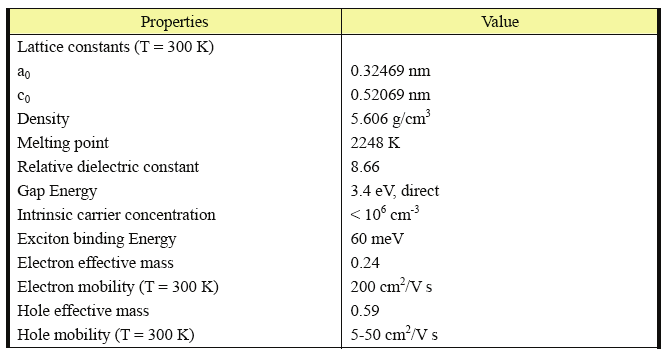
Table 1. Physical properties of wurtzite ZnO [Fan et al; Ref 8]
Zinc oxide has a hexagonal structure (space group P63mc) with lattice parameters a = 0.3296,
and c = 0.52065 nm. The structure of ZnO can be simply described as a number of
alternating planes composed of tetrahedral coordinated O2- and Zn2+ ions, stacked
alternatively along the c-axis (Figure 1a). The tetrahedral coordination in ZnO results in non-
central symmetric structure and piezoelectricity. Another important characteristic of ZnO is
the polar surfaces. The most common polar surface is the basal plane. The oppositely
charged ions produce positively charged Zn-(0001) and negatively charged O-(000 1 ) polar
surfaces (Figure 1b), resulting in a normal dipole moment and spontaneous polarization
along the c-axis.
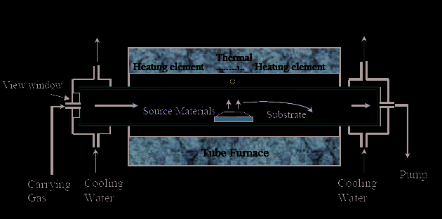
Another polar surface is the {01 1 1}. By projecting the structure along [1 2 10], as shown in
Figure 1b, beside the most typical ±(0001) polar surfaces that are terminated with Zn and
oxygen, respectively, ±(10 1 1) and ±(10 1 1 ) are also polar surfaces. The {10 1 1} type
surfaces are not common for ZnO, but they have been observed in a nanohelical structure
found recently [9]. The charges on the polar surfaces are ionic charges, which are non-
transferable and non-flowable. Because the interaction energy among the charges depends
ZnO Nanostructures for Optoelectronic Applications
175
on the distribution of the charges, the structure is arranged in such a configuration to
minimize the electrostatic energy. This is the main driving force for growing the polar
surface dominated nanostructures.
Fig. 1. (a) Wurtzite structure model of ZnO. The tetrahedral coordination of Zn-O is shown.
(b) The structure model of ZnO projected along [2 1 1 0], displaying the ±(0001), ± (01 1 1 )
and ± (01 1 1) polar surfaces
3. Growth of ZnO nanostructures
Growth of ZnO nanostructures has been carried out by several groups using the techniques
that are still being developed for their reliability and throughput. These approaches are
listed in three broad categories. These include:
1. Vapor Phase Deposition Technique ( Solid-Vapor Process) [10]
2. Chemical Synthesis Method [10]
3. Induction Heating Method [11]
4. Metal-Organic Chemical Vapor Deposition (MOCVD) [12,13]
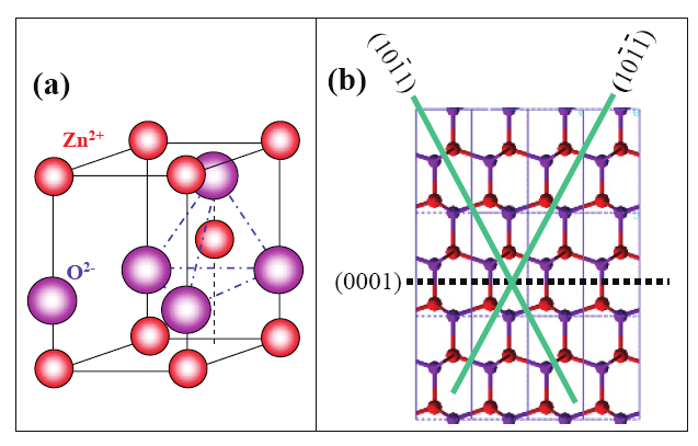
There are several processing parameters such as temperature, pressure, carrier gas
(including gas species and its flow rate), substrate and evaporation period, which can be
controlled and need to be selected properly before and/or during the thermal vaporization
[10]. The source temperature selection mainly depends on the volatility of the source
material(s). Usually, it is slightly lower than the melting point of the source material. The
pressure is determined according to the evaporation rate or vapor pressure of the source
material(s). The schematic representation of the Vapor Phase Deposition technique is shown
in figure 2.
The substrate temperature usually drops with the distance of its location from the position
of the source material(s). The local temperature determines the type of product that will be
obtained. It is also noted that the thermal evaporation process is very sensitive to the
concentration of oxygen in the growth system. Oxygen influences not only the volatility of
176
Optoelectronic Devices and Properties
the source material(s) and the stoichiometry of the vapor phase, but also the formation of
the product(s).
Fig. 2. A schematic diagram of the experimental apparatus for growth of oxides
nanostructures by the solid–vapor phase process [Wang et al; Ref 10]
The Second Growth approach for ZnO nanowires uses the chemical synthesis method [10].
This is a hydrothermal method, where the growth procedure for growth of ZnO nanowires
is as follows:1). Suspend the surface modified substrate in a Pyrex glass bottle filled with an
equal molar aqueous solution of zinc nitrate hydrate (Zn(NO3)2.6H2O) and
hexamethylenetetramine (C6H12N4) at temperatures between 60-90 C. 2). The temperature,
PH, solution concentration, reaction time (a range of 1-72 hours) and substrate surface status
were optimized for growing Nanowire arrays with controlled dimensions and orientation.
3). after completion of the reaction, the substrates were removed from the solution, and
rinsed by de-ionized water, and dried in air at 65 C.
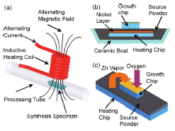
The third approach uses the inductive heating assisted fast synthesis of ZnO nanowires
using ZnO/graphite solid source powder in a room temperature environment [13]. The
internal heat generation induced by the alternating magnetic field at the synthesis specimen
enables the fast temperature transition for ZnO nanowire growth, with a synthesis time less
than 5 min compared to conventional methods. Furthermore, this demonstration illustrates
the feasibility of a simple and fast nanoscale synthesis using inductive heating for
nanomaterials synthesis [13].
Figure 3a shows the schematic illustration for the ZnO nanowire synthesis setup. The
synthesis specimen is placed inside a quartz tube underneath the center of an eight-turn
inductive coil with a pitch of 3.25 mm and an inner/outer diameter of 12.7/ 19.2 mm. The
distance between the coil base and the synthesis specimen is - 6 mm.
The cross sectional view of the synthesis specimen, including a nickel coated heating chip,
source powder, and growth chip inside a ceramic boat, is shown in Figure 3 b. When an
alternating current is applied in the coil, an alternating magnetic field is generated, which
induces eddy currents in the nickel layer and provides rapid Joule heating for nanowire
synthesis. Analytically, one can derive each coil’s magnetic field intensity generated at any
point with a scalar distance of d with respect to the coil loop center from Biot-Savart’s law
[Lin et al 2007; Ref 11].
ZnO Nanostructures for Optoelectronic Applications
177
Fig. 3. Schematic illustration for ZnO nanowire synthesis setup using induction heating
method (a). Cross sectional view of the synthesis specimen consisting of a heating chip,
source powder, and growth chips inside a ceramic boat (b). Three-dimensional sketch of the
heating chip/source powder/growth (c) [Lin et.al; Ref 11]
Several groups are have used Metal-Organic Chemical Vapor Deposition (MOCVD)
successfully to grow ZnO nanostructures and have shown good results [12, 13]. Further
work is underway to develop this technology for oriented ZnO nanowires for optoelectronic
applications.
4. Oriented nanostructures growth
For the first two growth approaches, selectively patterned substrates have been used to
control the density and selectivity of the aligned growth. The patterned materials can be
catalysts (Au, Ni, etc.). The patternings methods are Electron-beam Lithography and
Focused ion beam Microscopy.
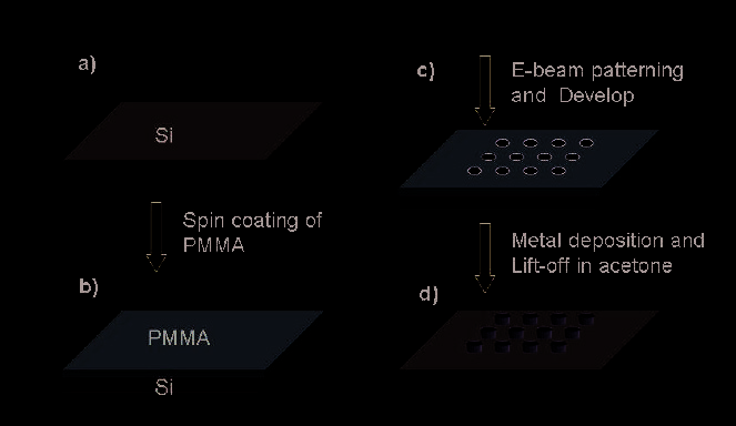
Figure 4 presents a standard process for E-beam lithography. First step is to spin-coat E-
beam resist PMMA of desired thickness layer on the substrate, and then using electron beam
to selectively expose the patterned area of PMMA coating. Next step is to develop the
exposed pattern using MIBK solution. After this step, the PMMA coating on the Si substrate
is left with a pattern, which is subsequently filled by metal deposition, and the remaining
PMMA can be lifted off in acetone.
This patterned substrate can be used for growth of ZnO nanowires. They are currently
developing the lift-off process to fabricate the substrates. Once the process is refined on
Silicon substrates, it can be further implemented on other substrates [10].
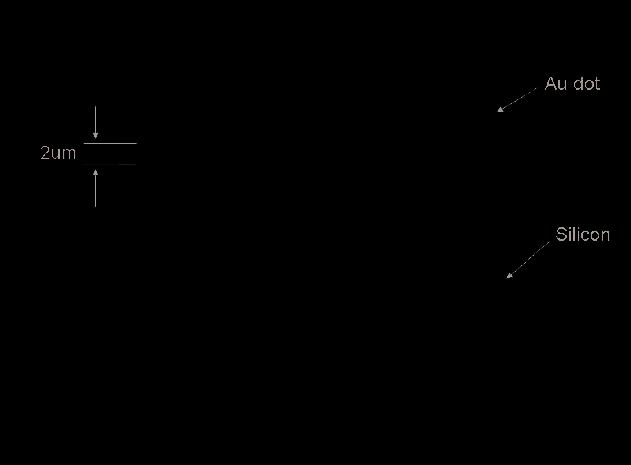
Figure 5 presents Au-pattern on Si substrate. We have recently achieved the Au-pattern
using E-beam lithography. The patterned gold dot array is 2 um in diameter, 2 um in
spacing, and 200 nm in height.
178
Optoelectronic Devices and Properties
Fig. 4. E-beam Lithography Process Flow for growth of ZnO Nanowires [Wang et al; Ref 10]
Fig. 5. Au Pattern on Silicon substrate with 20 micron size [Wang et al; Ref 10]
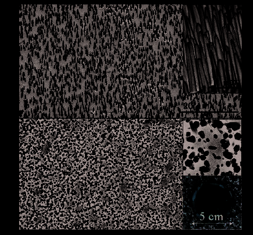
The hydrothermal synthesis method has been very successful in terms of synthesizing large
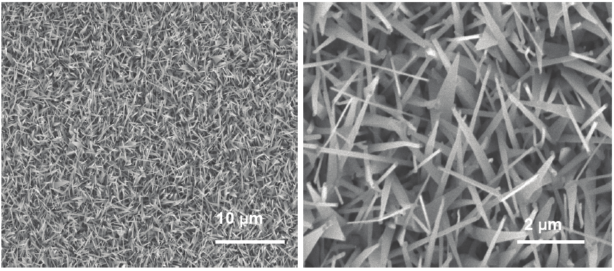
scale nanowires arrays on Silicon substrates. As shown in figure 6a is a side view SEM
image of the as grown ZnO nanowires arrays on Au-coated Si substrate, the alignment is
very good. The zoom-in image in the inset displayed the dimensions of the grown nanowire,
~200 nm in diameter, ~ 5 um in lengths.
ZnO Nanostructures for Optoelectronic Applications
179
Figure 6b shows the top view of aligned nanowire arrays; the top-right inset enlarged
picture clearly illustrated the hexagonal cross-section of the nanowires. The bottom-right
CCD image is showing a 2-inch diameter sized area of nanowires arrays grown on an Au-
coated substrate.
Fig. 6. ZnO Nanowires grown on Silicon Substrate [Wang et al; Ref 10]
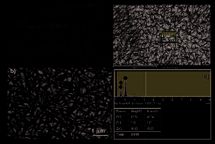
Besides Au, they have also evaluated the ZnO seeds for promoting growth of ZnO
nanowires using hydrothermal synthesis. As shown in figure 6a, a low-magnification SEM
image showing the growth of ZnO nanowires on ZnO seeds coated (30 nm in thickness)
PMMA film. The wavy feature is due to the non-uniform PMMA coating surface. The
enlarged top view was revealed in figure 6b, witnessing the randomly grown nanowires
with sharp tips ~20 nm in diameter. The EDS analysis in figures 6c-d revealed the main
composition of ZnO with some impurities. They have identified the impurity to be
Chromium (Figure 6d).
Density controls of nanowires growth are also being studied as an important parameter for
the UV detector and Sensor application. As shown in figure 7, a typical dispersive
nanowires array on Au-coated Si substrate. The wire diameter is about 1-2 um (figure 7 b),
the length can be as long as 30 um, and the spacing in between nanowires are ~5-15 um.
Figure 7c revealed the additional growth of nanoscale ZnO dots on the Si substrate
corresponding to the densely distributed nanodots in figure 7b, which might be the seeds
(nuclei) of ZnO nanowires growth.
180
Optoelectronic Devices and Properties
Fig. 7. ZnO nanowire growth on ZnO coated substrates [Wang et al; Ref 10]
Fig. 8. ZnO nanowires grown on SiC (0001) substrates with 2 nm Au at 960 C [Wang et al;
Ref 10]
They have also evaluated growth of ZnO nanowires on SiC substrates. SiC being a wide
bandgap semiconductor can be used for active device fabrication. For this effort, we have
used SiC (0001) substrates. We have used thermal evaporation method using ZnO and C as
source material. Au, 2-4 nm thick was used as a catalyst for the growth. We also used Argon
ZnO Nanostructures for Optoelectronic Applications
181
and Oxygen as the carrier gases. Figure 8 presents the ZnO nanowires and nanosheets on
SiC (0001) coated with 2 nm gold. The growth was carried out at 960 C, using Argon and
Oxygen. The growth was carried out for 30 minutes.
The results in figures 8 show their attempts to grow the ZnO nanowires. The process is still
being optimized for oriented growth with different growth te