Significant progress has been made in thin film solar cells that have demonstrated efficiency
in excess of 30 percent for GaAs based multijunction solar cells, which are being used for
space mission [39]. There are several different configurations that would allow high
efficiency solar cells. More recently, there is interest in using GaN / InGaN and ZnO /
MgZnO for development of high efficiency multijunction solar cells [40].
Fig. 17. Band gap energy for solar spectrum. Several material systems are being developed
to provide high efficiency multijunction solar cells. These include material components Ge,
GaAs and GaInP, InGaN and ZnO. [Wu et al; Reference 40]
Figure 17 presents complete solar spectrum for AM-1.5 solar cells. Different material
systems can be utilized to accomplish high efficiency multijunction solar cells. Most of the
multijunction solar cells have been developed for space missions where availability of high
efficiency is of paramount importance and issue of radiation hardness is critical success for
the space missions. There has been significant effort for development of low cost
technologies that will allow high efficiency thin film solar cells for terrestrial applications.
ZnO Nanostructures for Optoelectronic Applications
191
ZnO is being explored as one of the key components for a variety of low cost thin film and
nanostructure based solar cells. Recent work reported by Ganguly and his coworkers [41]
has explored the use of amorphous silicon solar cells with ZnO with insertion of
Germanium layers. They have shown that with insertion of a thin amorphous germanium
layer at the ZnO-p-layer interface improves the cell performance and diode ideality by
suppression of Oxygen and Zinc incorporation in the silicon layers. One of the advantages
of ZnO is is its resistance to hydrogen plasma induced darkening and higher transmission
thereby improving the solar cell efficiency.
Recent work by Peiro and his coworkers [36] at Imperial college and Manchester in UK have
shown that solar cells fabricated from composites of conjugated polymers with
nanostructure ZnO are of great interest for their stability, low cost and electron transport
properties. ZnO polymer solar cells are promising for low temperature synthesis.
Zinc oxide (ZnO)/polymer solar cells are promising compared to other metal
oxide/polymer combinations, on account of the possibility of low temperature synthesis, as
well as the potential for controlling interface morphology through simple processing from
solution. They have focused on the effect of surface morphology of ZnO films on
photovoltaic device performance. They have successfully grown ZnO nanorods standing
almost perpendicular to the electrodes on a flat, dense ZnO “backing” layer.
They have studied [ 36, 37] structures consisting of a conjugated polymer in contact with
three different types of ZnO layer: a flat ZnO backing layer alone; ZnO nanorods on a ZnO
backing layer; and ZnO nanoparticles on a ZnO backing layer. They also used scanning
electron microscopy, steady state and transient absorption spectroscopy and photovoltaic
device measurements to study the morphology, charge separation and recombination
behavior and device performance of the three types of structures.
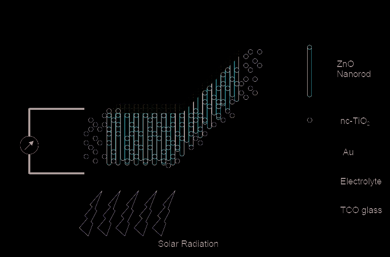
Fig. 18. Schematic diagram of ZnO based nanostructure solar cell [Sridhar et al; Ref 34]
They found that charge recombination in the structures containing vertically aligned ZnO
nanorods is remarkably slow, with a half life of over 1 ms, over two orders of magnitude
slower than for randomly oriented ZnO nanoparticles. A photovoltaic device based on the
nanorods structure which has been treated with an ambiphilic dye before deposition of
poly(3-hexyl thiophene) (P3HT) polymer shows a power conversion efficiency over four
times greater than for a similar device based on the nanoparticles structure.
192
Optoelectronic Devices and Properties
The best ZnO nanorods: P3HT device yields a short circuit current density of 2 mAcm-2
under AM1.5 illumination (100mWcm-2) and peak external quantum efficiency over 14%,
resulting in a power conversion efficiency of 0.20%. Their effort demonstrates the potential
of ZnO nanostructure based solar cells have the potential of low cost and further
improvements can yield higher efficiency solar cells.
Several other groups in US, China and England [34, 36, 41, 42] are working on ZnO
nanostructure solar cells. They are all trying to develop the necessary understanding for
growth and characterization of ZnO nanostructures on variety of substrates.
Investigation of ZnO nanorods based solar cells is being conducted towards developing
alternative, lightweight, flexible devices for commercial applications. A schematic view is
shown in figure 18 .A lot of research has been done in the area of dye sensitized solar cells [
37, 42] in particular, which is currently the most stable and efficient excitonic solar cell.
Aligned ZnO nanorods, with their high carrier mobilities serve as the conduction pathways
for the excitons. These approaches provide a glimpse of what is being done on using ZnO
nanostructures fro solar cell applications. Further effort is needed in developing ZnO based
solar cells that can be implemented in terrestrial applications.
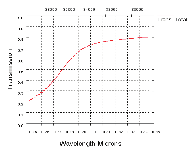
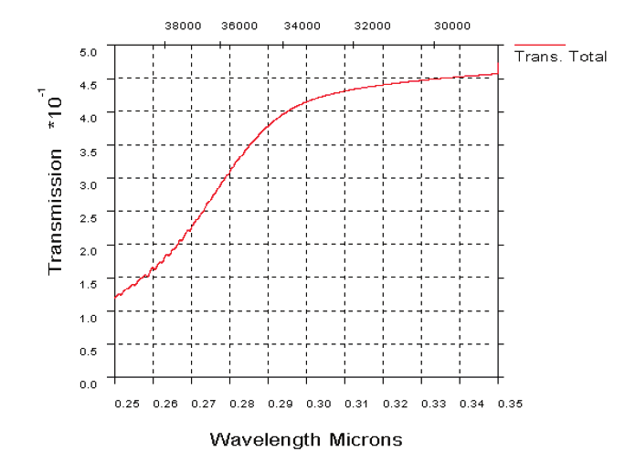
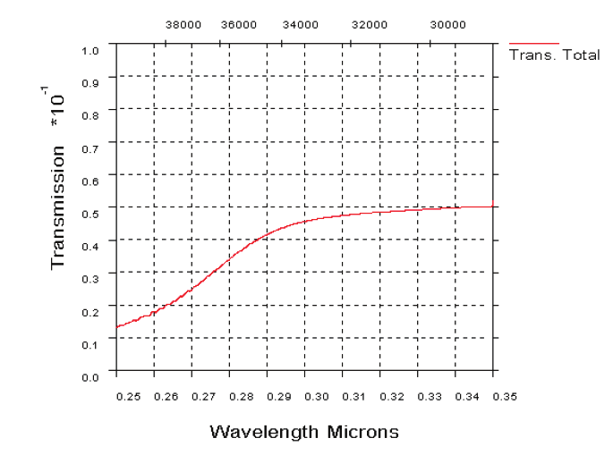
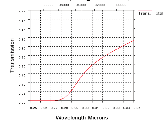
11. UV atmospheric transmission model
There has been recent effort to study the atmospheric transmission models in UV, Visible
and Infrared (IR) bands [43]. Modeling of atmospheric effects on transmission at UV
wavelengths (250-350 nm range) was performed using MODTRAN. MODTRAN
(MODerate resolution atmospheric TRANsmission) is an atmospheric radiative transfer
model that may be used to determine the effects of various atmospheric layers and weather
conditions on wavelength dependent free-space transmission. Six different atmospheric
models were simulated: clear maritime (23 km visibility), desert extinction, drizzle (2
mm/hr), light rain (5 mm/hr), moderate rain (12.5 mm/hr), and heavy rain (25 mm/hr).
(a)
(b)
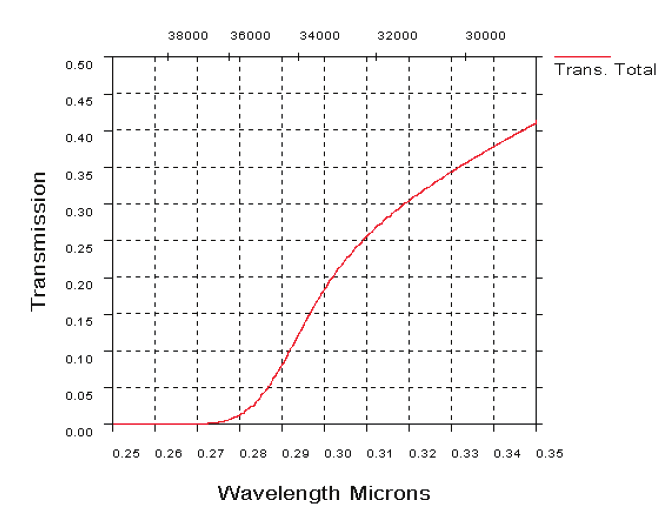
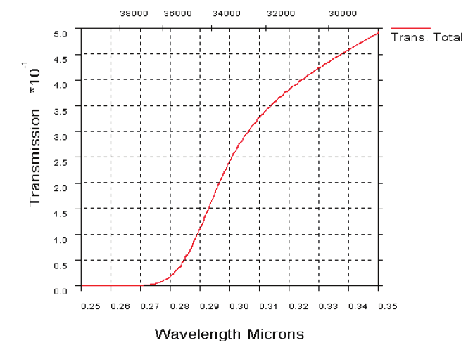
Fig. 19. UV atmospheric transmission over a horizontal path in clear maritime (23 km
visibility) conditions, 1 km range (19 a). UV transmission through atmosphere over a
horizontal path in desert extinction conditions, 1 km range (19b)
ZnO Nanostructures for Optoelectronic Applications
193
For each of these weather conditions, UV transmission was modeled for 1 km horizontal
paths through the atmosphere 5 m above the surface (Figures 1-6). In addition, slanted
paths at angles of 15º, 30º, 45º, and 60º from the horizon for a distance of 10 km were
simulated in clear maritime conditions (Figures 19-23) to show the relative effects of
propagation though different lower atmospheric layers on attenuation. In relation to free-
space optical communication networks, a 0º horizontal path would involve ground based
communication extending no further than the horizon, while an upward slanted path might
involve communication between a ground-based unit or sea vessel and an aircraft [43].
(a)
(b)
Fig. 20. UV atmospheric transmission over a horizontal path in drizzle (2 mm/hr)
conditions, 1 km range (20a) and UV transmission over a horizontal path in light rain (5
mm/hr) conditions, 1 km range (20b).
(a)
(b)
Fig. 21. UV transmission through atmosphere over a horizontal path in moderate rain (12.5
mm/hr) conditions, 1 km range (21a). UV transmission over a horizontal path in heavy rain
(25 mm/hr) conditions, 1 km range (21b)
194
Optoelectronic Devices and Properties
(a)
(b)
Fig. 22. UV atmospheric transmission over a slanted path at 15º elevation in clear maritime
conditions, 10 km range (22a). UV transmission over a slanted path at 30º elevation in clear
maritime conditions, 10 km range (22b)
(a)
(b)
Fig. 23. UV transmission over a slanted path at 45º elevation in clear maritime conditions, 10
km range (23a). UV atmospheric transmission over a slanted path at 60º elevation in clear
maritime conditions, 10 km range ( 23b)
12. Summary
In this chapter, we have discussed growth, fabrication and characterization of ZnO
nanostructures materials and devices on a variety of substrates. ZnO nanostructures offer
potential for a variety of optical, electronic and biological devices for nanoscale applications.
The Zinc oxide nanostructures are also attractive for energy generation devices and
photovoltaic applications. Significant research effort is underway on ZnO nanostructures,
their unique properties for application in transparent electronics, ultraviolet (UV) light
emitters, piezoelectric devices, chemical sensors and spin electronics.
ZnO Nanostructures for Optoelectronic Applications
195
An assortment of ZnO nanostructures, such as nanorods, nanotubes and nanorings, have
been successfully grown via a variety of methods including chemical vapor deposition,
thermal evaporation, hydrothermal technique, sol-gel and electro-deposition. These
nanostructures have been evaluated for electronic devices, UV detectors, light emitting
diodes, lasers, gas sensors, and other biological applications. Further work is underway that
will enhance our understanding of ZnO nanostructures and their applications for future
system applications.
13. Acknowledgement
The authors would like to acknowledge the contributions of many students at Georgia Tech
that have over the years contributed to the exciting work, which has been published by
them and presented here in the chapter. We would also like to acknowledge the modeling
effort by Dr. John Zeller of NUWC, Newport, RI. The authors would also like to
acknowledge the financial support by numerous agencies that have contributed to the ZnO
nanostructures and their applications.
14. References
[1] J. R. Choi and Dennis. L. Polla Journal of Micromechanical Micro-engineering Volume 3, 60-
64, 1993
[2] E. J. Egerton, A. K. Sood, R. Singh, Y. R. Puri, R. F. Davis, J. Pierce, D. C. Look and T.
Steiner, Journal of Electronic Materials Vol.34, No.6, 2005
[3] Z. L. Wang , A Review Paper, Journal of Physics: Condensed Matter 16, 829-858, 2004
[4] X. Wang, J. Song, C. J. Summers, J. H. Ryou, P. Li, R. D. Dupuis, and Z. L. Wang , J.
Phys. Chem. B, 110 (2006) 7720-7724
[5] X. Wang , J. Song , P. Li , J. H. Ryou , R. D. Dupuis , C. J. Summers and Z. L. Wang , J.
Am. Chem. Soc., 127 (2005) 7920-7923
[6] X. Wang, C. J. Summers and Z. L. Wang, Nano Letters, 3 (2004) 423-426.
[7] Z. L. Wang and J. Song, Science, 312 (2006) 242-246
[8] Z. Fan and J.G. Lu, Journal of Nanoscience and Nanotechnology, Volume 5, 1561-1573 (2003)
[9] R.S. Yang, Y. Ding and Z.L. Wang, Nano Lett. , 4, 1309 (2004)
[10] A.K. Sood, Y.R. Puri, P. Gao, C. Lao, Z.L. Wang, D.L. Polla, M.B. Soprano, Proceedings of
SPIE, Volume 6556, 6556IL ( 2007)
[11] L. Luo, B. Sosnowchik and L.W. Lin, Applied Physics Letters 90, 093101 (2007)
[12] W. Lee, M. C. Jeong and J.M. Myoung, Acta Materialia, 52, 3949-3957(2004)
[13] J. B. Baxter and E.S. Aydil, Journal of Electrochemical Society, 156 (1), H52-H58 (2009)
[14] P. X. Gao and Z. L. Wang, J. Phys. Chem. B 106, 12653 (2002)
[15] P. X. Gao, Y. Ding and Z. L. Wang, Nano Lett. 3, 1315 (2003)
[16] Z. W. Pan, Z. R. Dai and Z. L. Wang, Science 291, 1947(2001)
[17] M. H. Huang, Y. Y. Wu, H. Feick, N. Tran, E. Weber and P. D. Yang, Adv. Mater. 13, 113
(2001)
[18] M. S. Arnold, P.H. Avouris, Z. W. Pan and Z. L. Wang, J. Phys. Chem. B 107, 659 (2003)
[19] Y. Cui and C. M. Lieber, Science 291, 851 (2001)
[20] P. G. Collins, M. S. Arnold and Ph. Avouris, Science 292, 706 (2001)
[21] J. Kong, N. Franklin, C. Wu, S. Pan, K. J. Cho and H. Dai, Science 287, 622 (2000)
[22] Wang, X.D., Ding, Y. Summers, C.J. and Wang, Z.L., J. Phys. Chem. B. 108, 8773 (2004)
196
Optoelectronic Devices and Properties
[23] X. Bai, E. G. Wang , P. Gao and Z. L. Wang, NanoLetters, 3, 1147 (2003)
[24] P. M. Morales and C. M. Lieber, Science 279, 208 (1998)
[25] G.F. Zheng, F. Patolsky, Y. Cui, W.U. Wang, and C.M. Lieber, Nature Biotechnology 23
(2005) p. 1294
[26] X.D. Bai, P.X. Gao, Z.L. Wang and E.G. Wang, Appl. Phys. Letts. 82, p. 4806 ( 2003)
[27] Z. L. Wang, and J. H. Song, Science 312 , p. 242 ( 2006)
[28] J.H. Song, J. Zhou, and Z.L. Wang, Nano Lett. 6 p. 1656 ( 2006)
[29] M.H. Zhao, Z.L. Wang, and S.X. Mao, Nano Lett. 4 (2004) p. 587
[30] Z.L. Wang, X.Y. Kong, and J.M. Zuo, Phys. Rev. Letts. 91 (2003) p. 185502
[31] Z.L. Wang and J. H. Song, Science, 312 , 242-246 ( 2006)
[32] P.X. Gao, J.H. Song, J. Liu and Z.L. Wang, Advanced Materials, 19, 67-72 (2006)
[33] X.D. Wang, J.H. Song, J. Liu and Z.L. Wang, Science, 316, 102-105 ( 2007)
[34] D. Sridhar, J. Xie, J.K. Abraham, V. K. Varodan and S.H. Choi, Proceedings of SPIE,
Volume 6172 ( 2006)
[35] W. J. F. Beck, L. H. Slooft, M. J. Wienk, J. M. Kroon, and R.A. J. Janssen, Proceedings of
SPIE, Volume 5938 ( 2005)
[36] A. M. Piero, P. Ravirajan, K. Govender, D.S. Boyle, P.O. O’Brien, D.C. Bradley, J. Nelson
and J.R. Durrant, Proceedings of SPIE , Volume 5938 ( 2005)
[37] J. R. Baxter and E.S. Aydil, Applied Physics Letters, 86, 053114 (2005)
[38] For Silicon Solar Cells, i.e. Evergreen Solar (Marlboro, MA), Schott Solar (Burlington,
MA), and other Silicon Solar Cell Manufacturers). The cell efficiency varies from 14-
18 percent for Polysilicon to Single Crystal Silicon Solar Cells.
[39] T. Takamoto, E. Ikeda, H. Kurita and M. Ohmori, Applied Physics Letters, 70, 381 ( 1997)
[40] J. Wu, W. Walukiewicz, K. M. Yu, W. Shan, J. W. Ager, E.E. Haller, H. Lu, W.J. Schaff,
W.K. Metzer and S. Kurtz , Journal of Applied Physics, Volume 94, 6477 ( 2003)
[41] G. Ganguly, D.E. Carlson, S. S. Hyedus, D. Ryan , R. Gordon, D. Pang and R. C. Reedy,
Applied Physics Letters 85, p 479 ( 2004)
[42] Z. Longyue, D. Songyuan, X. Weiwei and K. Wang, Plasma Science and Technology,
Volume 8, No2, March 2006
[43] J. Zeller and T. Manzur, Proceedings of SPIE, Volume 7833, 783313 (2010)
10
Hybrid Optoelectronic and Photovoltaic
Materials based on Silicon Nanocrystals and
Conjugated Polymers
Vladimir Svrcek
Research Center for Photovoltaics,
National Institute of Advanced Industrial Science and Technology (AIST),
Central 2, Umezono 1-1-1, Tsukuba, 305-8568
Japan
1. Introduction
Hybrid material, which combines advantages of both organic and inorganic materials, might
offer potential for design of novel type of low cost devices with superior performance
(Schneider et al., 2000; Liu et al., 2008). The large choices for the organic and inorganic
structures offer the possibility to obtain materials with attractive physical and chemical
properties. The morphology of hybrid material at nanoscale might lead to very different
properties from crystalline solids. Particularly molecular structure polymers, conformation
and orientation can have a major effect on the macroscopic properties of novel material
(Coakley et la.,2003). Nanotubes are a promising subclass of nanomaterials owing unique
one-dimensional geometric features that can allow engineering the polymer based material
morphology at low cost. Nevertheless, nanotubes fabrication with diameter comparable
with exciton diffusion lengths of polymers (~ 15 nm) is still a problem. It has to be noted
that among the nanotubes with small diameter (< 5 nm), carbon-based discovered by Iijima
(Iijima 1991) were the first to gain recognition in academia (Marte et al., 2001; Harris, 2002;
Wang et al., 2009). Novel synthetic strategies for generating nanotubes from inorganic
materials have been recently also widely investigated and developed (Tenne et al., 1992;
Zhao, et al., 2004). It is believed that fiber/nanotube-polymer based arrays of material have
much lower reflectance and enable fabrication of thicker devices with increased absorption
compared with thin films.
One of the promising type of polymers used in variety of applications are the conjugated
conductive ones (Inzelt, 2008). It has to be noted that in traditional polymers e.g.
polyethylenes, the valence electrons are bound in sp3 hybridized covalent bonds (Inzelt,
2008). Therefore sigma-bond electrons have low mobility and do not contribute to the
electrical conductivity. Contrary to that conducting polymers have backbones of contiguous
sp2 hybridized carbon centers. As a result a valence electron on each center resides in a pz
orbital, which is orthogonal to the other three sigma-bonds. Then electrons within the band
become more mobile particularly when it is partially emptied. This advantage combined
with the mechanical properties (flexibility, toughness, malleability, etc.) make them
favorable also for optoelectronic applications as an active material.
198
Optoelectronic Devices and Properties
On the other hand, quantum dots, sometimes called as nanocrystals as well, are a special
class of semiconductor. They range in size from 2-10 nanometers in diameter. As a result the
excitons in quantum dots are confined in all three spatial dimensions (Murray, et al., 2000).
Particularly, silicon nanocrystals (Si-ncs) have many advantages over the other nanocrystal
materials (Canham, 1990; Hirsmman 1996). For instance, some of these materials contain
toxic elements such as lead or cadmium, and others rely on elements such as indium that are
in limited supply in nature. Silicon is no toxic and abundant. Newly observed phenomenon
in Si-ncs - so called multiple excitons generation - favorites Si-ncs as promising material for
photodetectors and solar cells (Beard,et al., 2007; Sukhovatkin et al., 2009). Namely the Si-nc
can produce two or three electrons per photon of high-energy sunlight and could lead to a
new type of solar cell with more than twice as efficient as nowadays used one. Colloidal Si-
ncs compared to solidly embedded in matrix allow easier processibility and fabrication of
device at low cost. [6] Free-standing Si-ncs and conjugated polymers blends shown be a
promising optoelectronic and photovoltaic composite material (Švrček et al., 2008a; Lui et
al., 2009).
In first part of this chapter we show that electrochemical etching and laser nanosecond laser
processing in liquid media is suitable for preparing doped (boron and phosphorus) colloidal
and surfactant free Si-ncs. Blends optoelectronic properties consisting of doped Si-ncs and
two conjugated polymers (e.g. (poly(3-hexylthiophene) (P3HT) and poly[methoxy-
ethylexyloxy-phenylenevinilene] (MEH PPV)) are discussed in details. It is demonstrated
that such Si-ncs can be successfully used for fabrication of room temperature
photoluminescent and photoconductive blends. The role of selected Si-ncs synthesis
techniques on the photoelectric properties of blends is compared. We argue that the
luminescence and transport properties of the blends are controlled by Si-ncs properties and
could be assigned to quantum confinement of excitons in Si-ncs. We demonstrate that the
transport properties of the blend can be tuned by processing conditions. The blends
containing Si-ncs produced by the laser ablation clearly evidence superior photovoltaic
properties due to the enhanced bulk-heterojunction surface area and improved charge
transport.
The morphology of the bulk-heterojunction can be significantly affected by various
fabrication parameters during the device formation. In second part of the chapter, in order
to achieve an efficient performance of the bulk-heterojunction, both the size distribution and
mesoscopic ordering of blend in nantubes is discussed. It is shown that a fiber- and/or
vertical 1D-like order of photosensitive bulk-heterojunction gives considerable advantages
over the thin film technology, because it provides larger interfacial area for efficient exciton
dissociation and straight path for photogenerated carries. As a result, fibers help to avoid
circuit shorts and interruption of percolation paths for carriers to their respective electrodes.
In this respect, a capillary induced filtering and assembly of blends in nanoporous templates
is discussed. We show that the titanium/alumina dioxide (TiO2/Al2O3) nanotubes template
could be suitable candidate for vertical order of photosensitive based blends.
2. Experimental methods
Colloidal and surfactant free Si-ncs with quantum confinements effects were prepared by
two independent techniques. First by electrochemical etching and second by laser ablation
of silicon wafer in water. For this purpose, boron-doped wafer with a resistivity of 0.5–
Hybrid Optoelectronic and Photovoltaic Materials based on
Silicon Nanocrystals and Conjugated Polymers
199
0.75Ocm (p-type, B concentration of 3x1016cm3) and phosphorous-doped wafer with a
resistivity of 0.5–2Ocm (n-type, P concentration 2x1016cm3) were used. The wafers were
electrochemically etched in a mixture of hydrofluoric acid with pure ethanol (HF:C2H5OH
1:4). In order to obtain a similar size distribution of Si-ncs, a constant current density 3.2
mA/cm2 and a constant etching time 60 min were used for the B-doped Si-ncs. In the case of
P-doped Si-ncs, we kept a constant current density at 1.6mA/cm2. In this process, the
etching time was 90 min and a halogen lamp illuminated the P-doped silicon substrate
during the electrochemical etching. The B- and P-doped and red luminescent Si-ncs were
harvested by mechanical scratching (Švrček et al., 2004). Second technique goes after the
synthesis route of blue luminescent Si-ncs based on a water-confined nanosecond laser
ablation process [Švrček et al., 2006; Švrček et al., 2009]. Particularly, the Si-ncs are prepared
by nanosecond excimer pulsed laser (KrF, 245 nm 20 Hz, 20 ns). Crystalline silicon doped
wafers with same charact